CY7C67300
Document #: 38-08015 Rev. *J Page 21 of 99
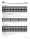
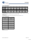
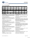
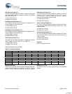
HSS Interrupt Enable (Bit 7)
The HSS Interrupt Enable bit enables or disables the following
High-speed Serial Interface hardware interrupts: HSS Block
Done and HSS RX Full.
1: Enable HSS interrupt
0: Disable HSS interrupt
In Mailbox Interrupt Enable (Bit 6)
The In Mailbox Interrupt Enable bit enables or disables the HPI:
Incoming Mailbox hardware interrupt.
1: Enable MBXI interrupt
0: Disable MBXI interrupt
Out Mailbox Interrupt Enable (Bit 5)
The Out Mailbox Interrupt Enable bit enables or disables the HPI:
Outgoing Mailbox hardware interrupt.
1: Enable MBXO interrupt
0: Disable MBXO interrupt
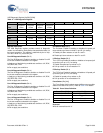
UART Interrupt Enable (Bit 3)
The UART Interrupt Enable bit enables or disables the following
UART hardware interrupts: UART TX, and UART RX.
1: Enable UART interrupt
0: Disable UART interrupt
GPIO Interrupt Enable (Bit 2)
The GPIO Interrupt Enable bit enables or disables the General
Purpose IO pins interrupt (see the GPIO Control Register
[0xC006] [R/W] on page 50).
When the GPIO bit is reset, all
pending GPIO interrupts are also cleared
1: Enable GPIO interrupt
0: Disable GPIO interrupt
Timer 1 Interrupt Enable (Bit 1)
The Timer 1 Interrupt Enable bit enables or disables the TImer1
Interrupt Enable. When this bit is reset, all pending Timer 1 inter-
rupts are cleared.
1: Enable TM1 interrupt
0: Disable TM1 interrupt
Timer 0 Interrupt Enable (Bit 0)
The Timer 0 Interrupt Enable bit enables or disables the TImer0
Interrupt Enable. When this bit is reset, all pending Timer 0 inter-
rupts are cleared.
1: Enable TM0 interrupt
0: Disable TM0 interrupt
Reserved
Write all reserved bits with ’0’.
Breakpoint Register [0xC014] [R/W]
Register Description
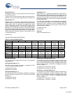
The Breakpoint register holds the breakpoint address. When the
program counter matches this address, the INT127 interrupt
occurs. To clear this interrupt, write a zero value to this register.
Address (Bits [15:0])
The Address field is a 16-bit field containing the breakpoint
address.
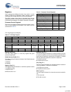
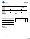
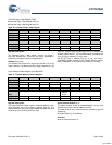
Table 30. Breakpoint Register
Bit # 15 14 13 12 11 10 9 8
Field Address...
Read/Write R/W R/W R/W R/W R/W R/W R/W R/W
Default 0 0 0 0 0 0 0 0
Bit # 7 6 5 4 3 2 1 0
Field ...Address
Read/Write R/W R/W R/W R/W R/W R/W R/W R/W
Default 0 0 0 0 0 0 0 0
[+] Feedback


