CY7C67300
Document #: 38-08015 Rev. *J Page 55 of 99
IDE PIO Port Registers [0xC050 - 0xC06F] [R/W]
All IDE PIO Port registers [0xC050 - 0xC06F] in Table 88 are defined in detail in the Information Technology-AT Attachment -4 with
Packet Interface Extension (ATA/ATAPI-4) Specification, T13/1153D Rev 18. The table Address column denotes the CY7C67300
register address for the corresponding ATA/ATAPI register. The IDE_nCS[1:0] field defines the ATA interface CS addressing bits and
the IDE_A[2:0] field define the ATA interface address bits. The combination of IDE_nCS and IDE_A are the ATA interface register
address.
HSS Registers
There are eight registers dedicated to HSS operation. Each of these registers are covered in this section and summarized in Table 89.
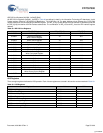
Table 88. IDE PIO Port Registers
Address ATA/ATAPI Register IDE_nCS[1:0] IDE_A[2:0]
0xC050 DATA Register ‘10’ ‘000’
0xC052 Read: Error Register
Write: Feature Register
‘10’ ‘001’
0xC054 Sector Count Register ‘10’ ‘010’
0xC056 Sector Number Register ‘10’ ‘011’
0xC058 Cylinder Low Register ‘10’ ‘100’
0xC05A Cylinder High Register ‘10’ ‘101’
0xC05C Device/Head Register ‘10’ ‘110’
0xC05E Read: Status Register
Write: Command Register
‘10’ ‘111’
0xC060 Not Defined ‘01’ ‘000’
0xC062 Not Defined ‘01’ ‘001’
0xC064 Not Defined ‘01’ ‘010’
0xC066 Not Defined ‘01’ ‘011’
0xC068 Not Defined ‘01’ ‘100’
0xC06A Not Defined ‘01’ ‘101’
0xC06C Read: Alternate Status Register
Write: Device Control Register
‘01’ ‘110’
0xC06E Not Defined ‘01’ ‘111’
Table 89. HSS Registers
Register Name Address R/W
HSS Control Register 0xC070 R/W
HSS Baud Rate Register 0xC072 R/W
HSS Transmit Gap Register 0xC074 R/W
HSS Data Register 0xC076 R/W
HSS Receive Address Register 0xC078 R/W
HSS Receive Length Register 0xC07A R/W
HSS Transmit Address Register 0xC07C R/W
HSS Transmit Length Register 0xC07E R/W
[+] Feedback


