


IXD1110 Demo Board
20 Development Kit Manual
Document Number: 250807
Revision Number: 003
Revision Date: June 27, 2003
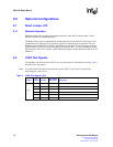
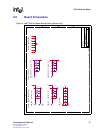
8.0 Test Points
8.1 Reset Test Points
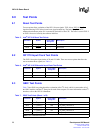
Two test points allow evaluation of the IXF1110 reset signals. TP21 allows IXF1110 Sys_Res
signal monitoring. DTP3 allows board reset signal monitoring. The board Sys_Res
can be
monitored on both test points if it is asserted by Switch S1 or the CPU. The reset is seen at TP21 if
an IXF1110 reset is issued by the software interface.
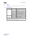
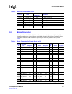
8.2 IXF1110 Input Clock Test Points
The IXF1110 requires input clocks of 50 and 125 MHz. There are two test points that allow the
user to monitor those signals (see Table 6).
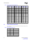
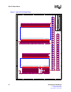
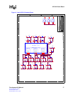
8.3 GBIC Test Points
Table 7 lists GBIC test points that allow evaluation of the I
2
C clock, which is connected to all of
the GBIC modules, and the I
2
C Data pins for each of the ten ports. For more information on the I
2
C
interface, refer to the IXF1110 Datasheet.
Table 5. Intel
®
IXF1110 Reset Test Points
Test Point Symbol
IXF1110 Ball
Designator
Description
TP21 Sys_Res
Y4 System reset for IXF1110
DTP3 Sys_Res
– Board reset
NOTE: DTP = Differential Test Point, TP = Test Point
Table 6. Intel
®
IXF1110 Differential Input Clock Test Points
Test Point Symbol
IXF1110 Ball
Designator
Description
DTP1 CLK125 AA5 125 MHz input clock for IXF1110
DTP2 CLK50 C21 50 MHz input clock for IXF1110
NOTE: DTP = Differential Test Point
Table 7. GBIC Test Points (Sheet 1 of 2)
Test Point Symbol
IXF1110 Ball
Designator
Description
DTP6 I
2
C_CLK L19 I
2
C_CLK for IXF1110
DTP7 I
2
C_DATA_0 G22 I
2
C_DATA_0 for IXF1110
DTP8 I
2
C_DATA_1 G23 I
2
C_DATA_1 for IXF1110
DTP9 I
2
C_DATA_2 J24 I
2
C_DATA_2 for IXF1110
DTP10 I
2
C_DATA_3 F22 I
2
C_DATA_3 for IXF1110
NOTE: DTP = Differential Test Point