


App. - 41 App. - 41
MELSEC-Q
APPENDIX
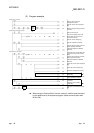
Appendix 9.6 When clearing received data
The following program example uses the receive data clear request area of the buffer
memory.
Refer to Section 6.1.4 for received data clear.
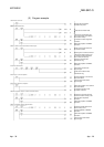
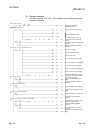
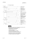
(1) Program conditions
The following program clears the received data in the OS area of the QJ71C24N
when the receive clear command (X1025) turns ON.
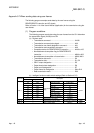
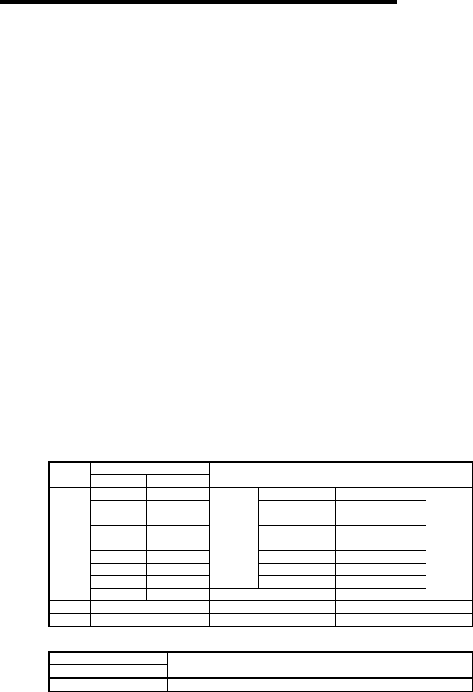
(a) Devices used
:
• Receive clear command......................................................... X1025
• Receive clear processing execution command ..................... M10
• Receive processing flag.......................................................... M11
• Transmission processing flag................................................. M12
• Receive clear command pulse signal .................................... M15
• Receive clear acceptance flag ............................................... M16
• Receive clearing flag............................................................... M17
• Communication disable flag ................................................... M18
• Communication enable flag.................................................... M19
• Completion check flag ............................................................ M20
• Receive clear processing execution status acquisition
command ................................................................................ M21
• Receive clear processing execution status judgment
command ................................................................................ M22
• Completion device for REMFR/REMTO instruction .............. M100 to 103
• Normal/abnormal completion flag for REMFR/REMTO
instruction................................................................................ M200, M201
• Receive data clear request area information......................... D0
• Clear request........................................................................... D1
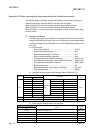
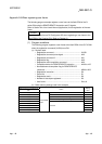
(b) Intelligent function module switch settings (Refer to Section 4.5.2)
Bit
Switch No.
Position Designated value
Description
Setting
value
b0 OFF Operation setting Independent
b1 OFF Data bit 7 bits
b2 OFF Parity bit No
b3 OFF Even/odd parity Odd
b4 OFF Stop bit 1 bit
b5 OFF Sum check code No
b6 ON Write during RUN Enabled
b7 ON
Transmission
setting
Setting modifications Enabled
Switch 1
b8 to b15 — Communication rate setting 19200bps
07C0
H
Switch 2 — Communication protocol setting Non-procedure protocol 0006
H
Switch 5 — Station number setting Station 0 0000
H
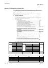
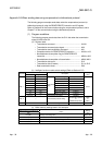
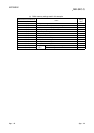
(c) Buffer memory settings used in this example
Address Decimal (Hexadecimal)
CH1
Name
Setting
value
168 (A8
H
) Receive data clear request 0, 1