


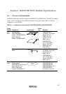
123
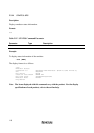
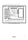
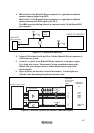
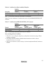
3. #RES of pin 4 of the Hitachi-UDI port connector is a signal line in which the
emulator outputs signals to the MCU.
#RES of pin 7 of the Hitachi-UDI port connector is a signal line in which the
emulator monitors the #RES signal of the MCU.
The #RES must be pulled up before it is connected to pin 7 of the Hitachi-UDI
port connector.
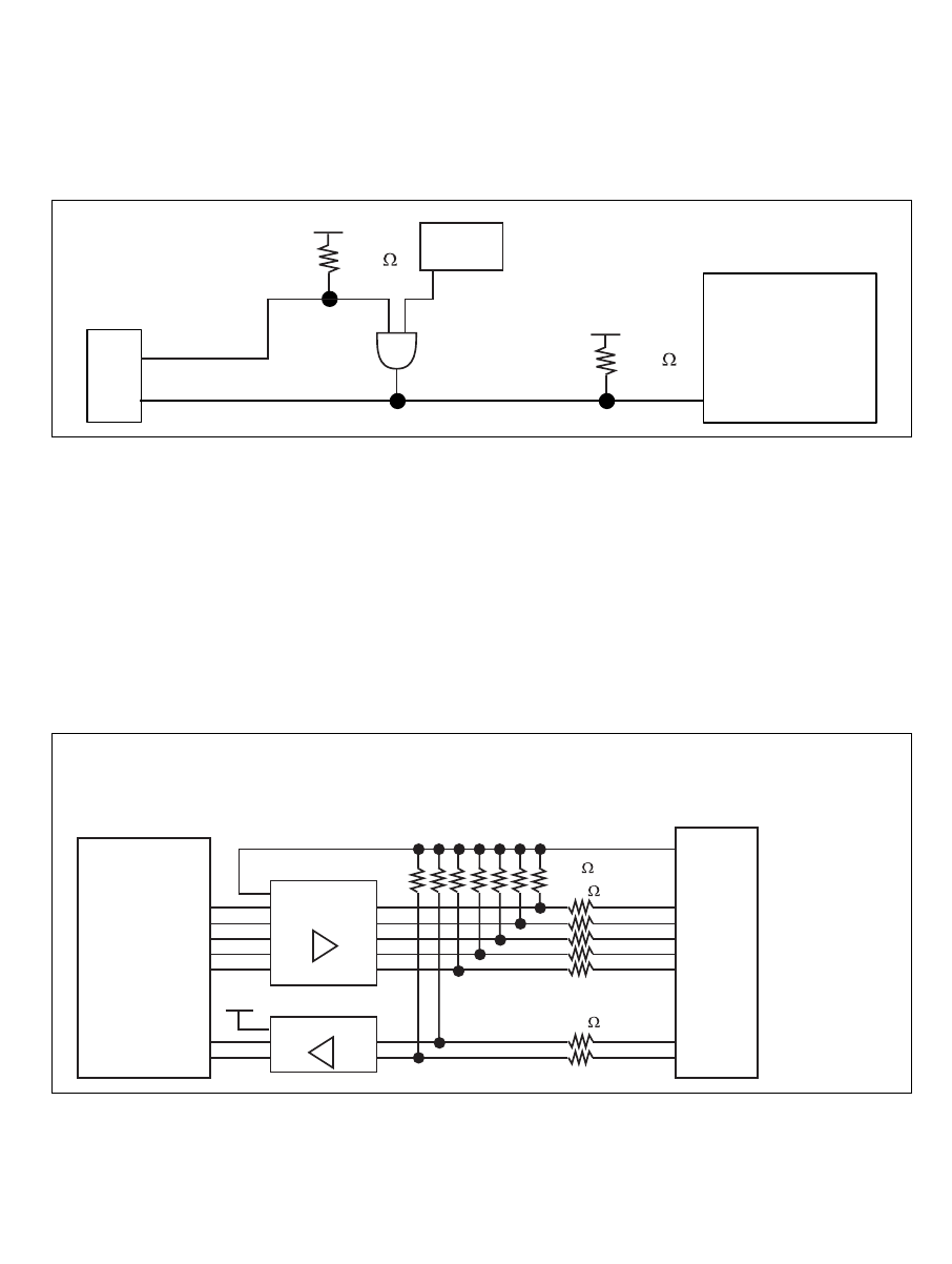
Hitachi-UDI
port connector
Pin 4
Pin 7
User
logic
4.7 k
H8S/2377F, H8S/2367F
Vcc
Vcc
4.7 k
Figure 6.5 Connection of #RES Pin
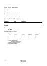
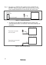
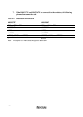
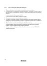
4. Connect GND of pins 8 to 10 and 12 to 14 in the Hitachi-UDI port connector to
GND in the user system.
5. Connect Vcc, pin 11 in the Hitachi-UDI port connector, to the power supply
(Vcc) in the user system. The amount of voltage permitted to input to the
Hitachi-UDI port connector must be within the guaranteed range of the
microcomputer.
6. Figure 6.6 shows the interface circuit in the emulator. Use this figure as a
reference when determining the pull-up resistance value.
Emulator control circuit
22 k
x 2
22 k
x 5
4.7 k
x 7
Hitachi-UDI
port connector
on the user
sytem
HD74LV125A
HD74LVTH244
Vcc
11
1
2
4
5
6
3
7
H8S/2377F,
H8S/2367F
Vcc
PG4
P53
#RES
PG5
PG6
#WDTOVF
#RES
Vcc
Vcc
3.3V
Figure 6.6 Interface Circuit in the Emulator (Reference Figure)