


M306H7T3-RPD-E User’s Manual 4. Hardware Specifications
REJ10J0964-0100 Rev.1.00 August 01, 2005 Page 72 of 88
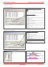
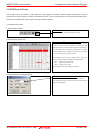
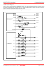
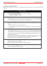
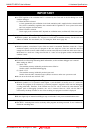
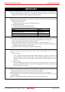
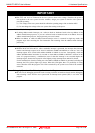
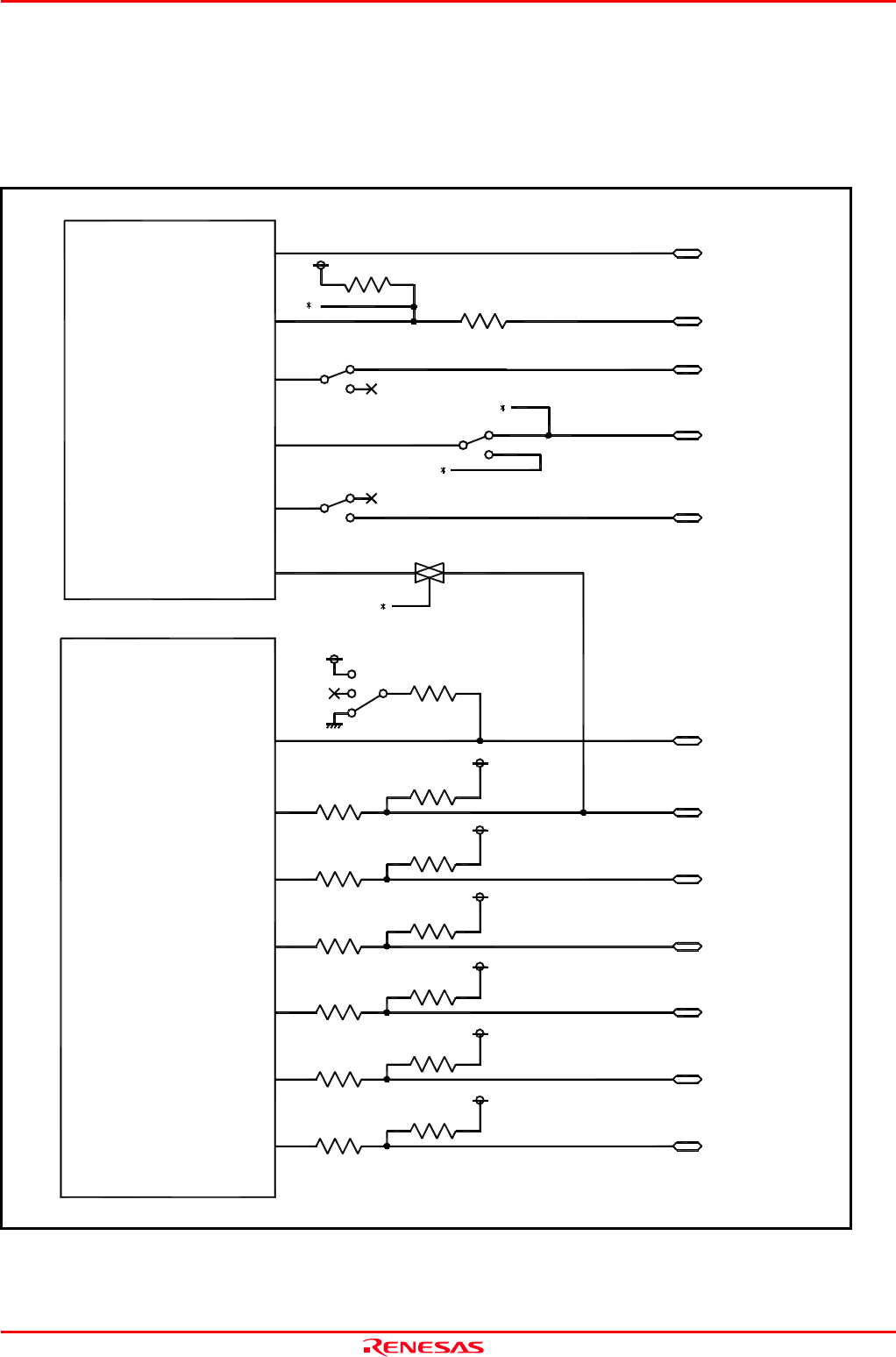
4.3 Connection Diagram
Figure 4.1 shows a connection diagram of the M306H7T3-RPD-E. This connection diagram mainly shows the interface section.
The circuits not connected to the user system such as the emulator's control system are omitted. The signals not shown in
Figure 4.1 connect the evaluation MCU and the user system directly.
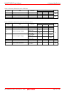
Tables 4.3 to 4.4 show IC electric characteristics of this product for reference purposes.
Figure 4.1 Part of the connection diagram of the M306H7T3-RPD-E
M306H7FG-TOOL(IC8)
I/O Emulate MCU
P60--P67
P70--P77
P80--P84
P90--P97
P85/NMI
100Ω
P86/Xcout
P85/NMI
P86/Xcout
OPEN
SW5
P86/Xcout
SW3
P87
P87/Xcin
P87/Xcin
Xcin
SW4
OPEN
Xout
Xout
CNVSS
1KΩ
SW2
P62F2(IC4)
Port Emulate FPGA
P00--P07
P00--P07
33Ω
RM1
Socket mounted
33Ω
Socket mounted
RM2
P10--P17
P10--P17
33Ω
P20--P27
Socket mounted
RM3
P20--P27
Socket mounted
33Ω
P30--P37
P30--P37
RM4
33Ω
P40--P47
Socket mounted
P40--P47
RM5
33Ω
P50--P57
Socket mounted
P50--P57
RM6
100KΩ
Xout
CNVSS
P90--P97
P80--P84
P70--P77
P60--P67
AN00--AN07
VDDIO
VDDIO
VDD2
VDD2
VDD2
VDD2
VDD2
VDD2
74HC4066