


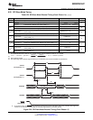


t
c(SPC)
+ SPI clock cycle time +
LSPCLK
4
or
LSPCLK
(SPIBRR )1)
+ t
c(LCO)
+ LSPCLK cycle time
20
15
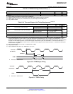
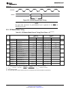
SPISIMO
SPISOMI
SPICLK
(clock polarity = 1)
SPICLK
(clock polarity = 0)
SPISIMO Data
Must Be Valid
SPISOMI Data Is Valid
19
16
14
13
12
SPISTE
(see Note A)
(2)
SM320F2812-HT
www.ti.com
SGUS062A–JUNE 2009–REVISED APRIL 2010
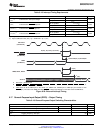
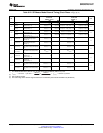
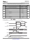
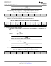
6.20 SPI Slave Mode Timing
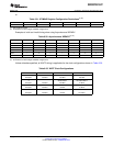
Table 6-23. SPI Slave Mode External Timing (Clock Phase = 0)
(1) (2) (3)
NO. MIN MAX UNIT
12 t
c(SPC)S
Cycle time, SPICLK 4t
c(LCO)
(2)
ns
t
w(SPCH)S
Pulse duration, SPICLK high (clock polarity = 0) 0.5t
c(SPC)S
– 10 0.5t
c(SPC)S
13
(4)
ns
t
w(SPCL)S
Pulse duration, SPICLK low (clock polarity = 1) 0.5t
c(SPC)S
– 10 0.5t
c(SPC)S
t
w(SPCL)S
Pulse duration, SPICLK low (clock polarity = 0) 0.5t
c(SPC)S
– 10 0.5t
c(SPC)S
14
(4)
ns
t
w(SPCH)S
Pulse duration, SPICLK high (clock polarity = 1) 0.5t
c(SPC)
– 10 0.5t
c(SPC)S
Delay time, SPICLK high to SPISOMI valid
t
d(SPCH-SOMI)S
0.375t
c(SPC)S
– 10
(clock polarity = 0)
15
(4)
ns
t
d(SPCL-SOMI)S
Delay time, SPICLK low to SPISOMI valid (clock polarity = 1) 0.375t
c(SPC)S
– 10
Valid time, SPISOMI data valid after SPICLK low
t
v(SPCL-SOMI)S
0.75t
c(SPC)S
(clock polarity = 0)
16
(4)
ns
Valid time, SPISOMI data valid after SPICLK high
t
v(SPCH-SOMI)S
0.75t
c(SPC)S
(clock polarity = 1)
t
su(SIMO-SPCL)S
Setup time, SPISIMO before SPICLK low (clock polarity = 0) 0
19
(4)
ns
t
su(SIMO-SPCH)S
Setup time, SPISIMO before SPICLK high (clock polarity = 1) 0
Valid time, SPISIMO data valid after SPICLK low
t
v(SPCL-SIMO)S
0.5t
c(SPC)S
(clock polarity = 0)
20
(4)
ns
Valid time, SPISIMO data valid after SPICLK high
t
v(SPCH-SIMO)S
0.5t
c(SPC)S
(clock polarity = 1)
(1) The MASTER/SLAVE bit (SPICTL.2) is cleared and the CLOCK PHASE bit (SPICTL.3) is cleared.
(3) Not production tested.
(4) The active edge of the SPICLK signal referenced is controlled by the CLOCK POLARITY bit (SPICCR.6).
A. In the slave mode, the SPISTE signal should be asserted low at least 0.5tc(SPC) before the valid SPI clock edge and
remain low for at least 0.5tc(SPC) after the receiving edge (SPICLK) of the last data bit.
Figure 6-26. SPI Slave Mode External Timing (Clock Phase = 0)
Copyright © 2009–2010, Texas Instruments Incorporated Electrical Specifications 113
Submit Documentation Feedback
Product Folder Link(s): SM320F2812-HT