


SM320F2812-HT
SGUS062A–JUNE 2009–REVISED APRIL 2010
www.ti.com
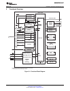
memory such that the vector table is fetched externally. The Boot ROM is disabled in this mode. In
microcomputer mode, Zone 7 is disabled such that the vectors are fetched from Boot ROM. This allows
the user to either boot from on-chip memory or from off-chip memory. The state of the XMP/MC signal on
reset is stored in an MP/MC mode bit in the XINTCNF2 register. The user can change this mode in
software and hence control the mapping of Boot ROM and XINTF Zone 7. No other memory blocks are
affected by XMP/MC.
I/O space is not supported on the F2812 XINTF.
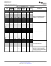
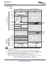
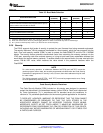
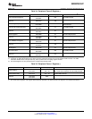
The wait states for the various spaces in the memory map area are listed in Table 3-2.
Table 3-2. Wait States
AREA WAIT-STATES COMMENTS
M0 and M1 SARAMs 0-wait Fixed
Peripheral Frame 0 0-wait Fixed
0-wait (writes)
Peripheral Frame 1 Fixed
2-wait (reads)
0-wait (writes)
Peripheral Frame 2 Fixed
2-wait (reads)
L0 and L1 SARAMs 0-wait
Programmable, Programmed via the Flash registers. 1-wait-state operation is possible at a reduced
OTP (or ROM)
1-wait minimum CPU frequency. See Section 3.2.6, Flash (F281x Only), for more information.
Programmed via the Flash registers. 0-wait-state operation is possible at reduced
Programmable,
Flash (or ROM) CPU frequency. The CSM password locations are hardwired for 16 wait-states.
0-wait minimum
See Section 3.2.6, Flash (F281x Only), for more information.
H0 SARAM 0-wait Fixed
Boot-ROM 1-wait Fixed
Programmed via the XINTF registers.
Programmable,
XINTF Cycles can be extended by external memory or peripheral.
1-wait minimum
0-wait operation is not possible.
30 Functional Overview Copyright © 2009–2010, Texas Instruments Incorporated
Submit Documentation Feedback
Product Folder Link(s): SM320F2812-HT