


SM320F2812-HT
SGUS062A–JUNE 2009–REVISED APRIL 2010
www.ti.com
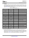
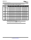
6.2 Recommended Operating Conditions
See
(1)
MIN NOM MAX UNIT
V
DDIO
Device supply voltage, I/O 3.14 3.3 3.47 V
1.8 V (135 MHz) 1.71 1.8 1.89
V
DD
, V
DD1
Device supply voltage, CPU V
1.9 V (150 MHz) 1.81 1.9 2
V
SS
Supply ground 0 V
V
DDA1
, V
DDA2
,
ADC supply voltage 3.14 3.3 3.47 V
AV
DDREFBG
, V
DDAIO
Flash programming supply
V
DD3VFL
3.14 3.3 3.47 V
voltage
V
DD
= 1.9 V ± 5% 2 150
Device clock frequency
f
SYSCLKOUT
MHz
(system clock)
V
DD
= 1.8 V ± 5% 2 135
All inputs except XCLKIN 2 V
DDIO
V
IH
High-level input voltage V
XCLKIN (at 50 mA max) 0.7V
DD
V
DD
All inputs except XCLKIN 0.8
V
IL
Low-level input voltage V
XCLKIN (at 50 mA max) 0.3V
DD
High-level output source All I/Os except Group 2 –4
I
OH
current, mA
Group 2
(2)
–8
V
OH
= 2.4 V
All I/Os except Group 2 4
Low-level output sink current,
I
OL
mA
V
OL
= V
OL
MAX
Group 2
(2)
8
T
A
Ambient temperature –55 25 220 °C
(1) See Section 6.7 for power sequencing of V
DDIO
, V
DDAIO
, V
DD
, V
DDA1
/V
DDA2
/AV
DDREFBG
, and V
DD3VFL
.
(2) Group 2 pins are as follows: XINTF pins, PDPINTA, TDO, XCLKOUT, XF, EMU0, and EMU1.
In Revision C, EVA (GPIOA0–GPIOA15) and GPIOD0 are 4 mA drive.
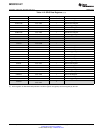
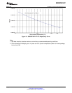
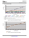
6.3 Electrical Characteristics
Over recommended operating conditions (unless otherwise noted)
(1)
PARAMETER TEST CONDITIONS MIN TYP MAX UNIT
I
OH
= I
OH
MAX 2.4
V
OH
High-level output voltage V
V
DDIO
I
OH
= 50 mA
– 0.2
V
OL
Low-level output voltage I
OL
= I
OL
MAX 0.4 V
All I/Os
(2)
(including XRS)
–80 –140 –190
V
DDIO
= 3.3 V,
Input
except EVB
With pullup
V
IN
= 0 V
I
IL
current mA
GPIOB/EVB –13 –25 –35
(low level)
With pulldown V
DDIO
= 3.3 V, V
IN
= 0 V ±2
Input With pullup V
DDIO
= 3.3 V, V
IN
= V
DD
±2
current
I
IH
mA
V
DDIO
= 3.3 V,
(high
With pulldown
(3)
28 50 80
V
IN
= V
DD
level)
Output current,
I
OZ
V
O
= V
DDIO
or 0 V ±2 mA
high-impedance state (off-state)
C
I
Input capacitance 7 pF
C
o
Output capacitance 7 pF
(1) Minimum and maximum parameters are characterized for operation at T
A
= 220°C unless otherwise noted, but may not be production
tested at that temperature. Production test limits with statistical guardbands are used to ensure high temperature performance.
(2) The following pins have no internal PU/PD: GPIOE0, GPIOE1, GPIOF0, GPIOF1, GPIOF2, GPIOF3, GPIOF12, GPIOG4, and GPIOG5.
(3) The following pins have an internal pulldown: XMP/MC, TESTSEL, and TRST.
86 Electrical Specifications Copyright © 2009–2010, Texas Instruments Incorporated
Submit Documentation Feedback
Product Folder Link(s): SM320F2812-HT