


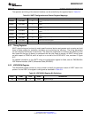
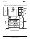
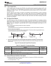
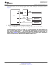

External Clock Signal
(Toggling 0−V
DD
)
C
b1
(see Note A)
X2X1/XCLKIN X1/XCLKIN X2
Crystal
C
b2
(see Note A)
(a) (b)
NC
SM320F2812-HT
www.ti.com
SGUS062A–JUNE 2009–REVISED APRIL 2010
3.8.1 Loss of Input Clock
In PLL enabled mode, if the input clock XCLKIN or the oscillator clock is removed or absent, the PLL still
issues a limp-mode clock. The limp-mode clock continues to clock the CPU and peripherals at a typical
frequency of 1 MHz to 4 MHz. The PLLCR register should have been written to with a non-zero value for
this feature to work.
Normally, when the input clocks are present, the watchdog counter decrements to initiate a watchdog
reset or WDINT interrupt. However, when the external input clock fails, the watchdog counter stops
decrementing (i.e., the watchdog counter does not change with the limp-mode clock). This condition could
be used by the application firmware to detect the input clock failure and initiate necessary shut-down
procedure for the system.
3.9 PLL-Based Clock Module
The F2812 has an on-chip, PLL-based clock module. This module provides all the necessary clocking
signals for the device, as well as control for low-power mode entry. The PLL has a 4-bit ratio control to
select different CPU clock rates. The watchdog module should be disabled before writing to the PLLCR
register. It can be re-enabled (if need be) after the PLL module has stabilized, which takes 131 072
XCLKIN cycles.
The PLL-based clock module provides two modes of operation:
• Crystal operation
This mode allows the use of an external crystal/resonator to provide the time base to the device.
• External clock source operation
This mode allows the internal oscillator to be bypassed. The device clocks are generated from an
external clock source input on the X1/XCLKIN pin.
A. TI recommends that customers have the resonator/crystal vendor characterize the operation of their device with the
DSP chip. The resonator/crystal vendor has the equipment and expertise to tune the tank circuit. The vendor can also
advise the customer regarding the proper tank component values that ensures start-up and stability over the entire
operating range.
Figure 3-8. Recommended Crystal/Clock Connection
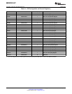
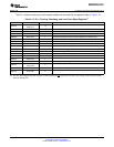
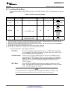
Table 3-15. Possible PLL Configuration Modes
PLL MODE REMARKS SYSCLKOUT
Invoked by tying XPLLDIS pin low upon reset. PLL block is completely disabled. Clock input
PLL Disabled XCLKIN
to the CPU (CLKIN) is directly derived from the clock signal present at the X1/XCLKIN pin.
Default PLL configuration upon power-up, if PLL is not disabled. The PLL itself is bypassed.
PLL Bypassed However, the /2 module in the PLL block divides the clock input at the X1/XCLKIN pin by XCLKIN/2
two before feeding it to the CPU.
Achieved by writing a non-zero value n into PLLCR register. The /2 module in the PLL block
PLL Enabled (XCLKIN × n) / 2
now divides the output of the PLL by two before feeding it to the CPU.
3.10 External Reference Oscillator Clock Option
The typical specifications for the external quartz crystal for a frequency of 30 MHz are listed below:
• Fundamental mode, parallel resonant
• C
L
(load capacitance) = 12 pF
Copyright © 2009–2010, Texas Instruments Incorporated Functional Overview 49
Submit Documentation Feedback
Product Folder Link(s): SM320F2812-HT