


SM320F2812-HT
SGUS062A–JUNE 2009–REVISED APRIL 2010
www.ti.com
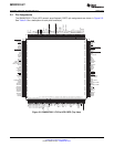
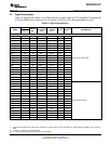
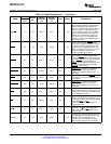
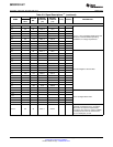
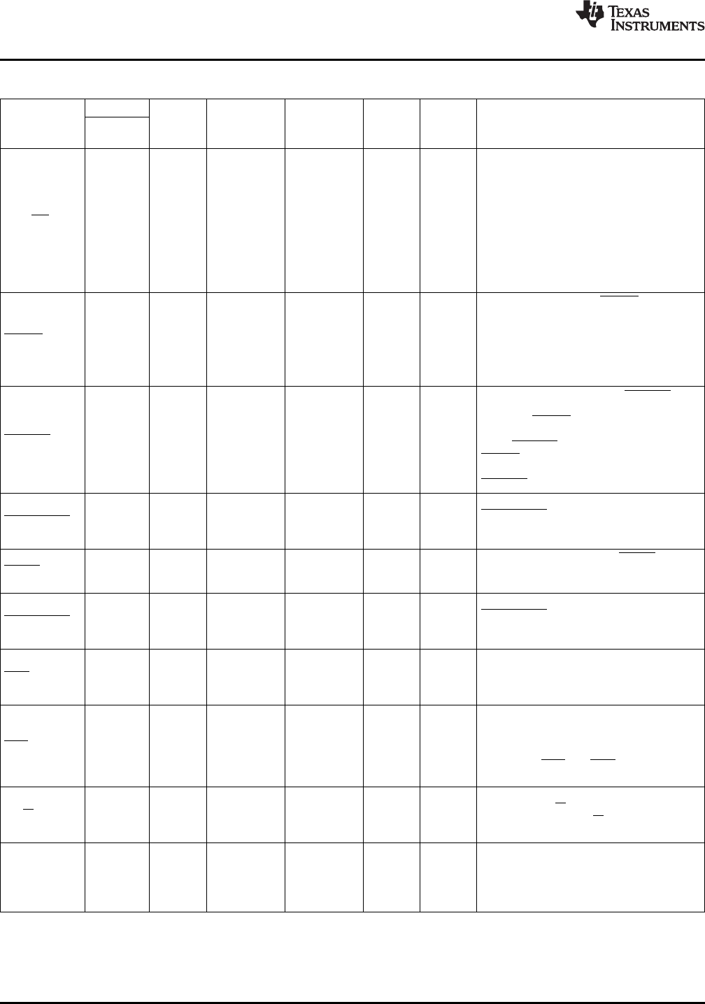
Table 2-3. Signal Descriptions
(1)
(continued)
PIN NO.
DIE PAD DIE PAD
DIE PAD
NAME X-CENTER Y-CENTER I/O/Z
(2)
PU/PD
(3)
DESCRIPTION
172-PIN
NO.
(mm) (mm)
HFG
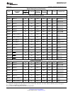
Microprocessor/Microcomputer Mode
Select. Switches between microprocessor
and microcomputer mode. When high,
Zone 7 is enabled on the external interface.
When low, Zone 7 is disabled from the
XMP/MC 17 23 2308.2 42.6 I PD external interface and on-chip boot ROM
may be accessed instead. This signal is
latched into the XINTCNF2 register on a
reset and the user can modify this bit in
software. The state of the XMP/MC pin is
ignored after reset.
External Hold Request. XHOLD, when
active (low), requests the XINTF to release
the external bus and place all buses and
XHOLD 155 174 42.6 2157.6 I PU strobes into a high-impedance state. The
XINTF releases the bus when any current
access is complete and there are no
pending accesses on the XINTF.
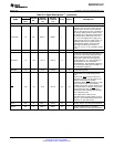
External Hold Acknowledge. XHOLDA is
driven active (low) when the XINTF has
granted a XHOLD request. All XINTF buses
and strobe signals are in a high-impedance
XHOLDA 80 93 5361.5 4137.4 O/Z –
state. XHOLDA is released when the
XHOLD signal is released. External devices
should only drive the external bus when
XHOLDA is active (low).
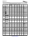
XINTF Zone 0 and Zone 1 Chip Select.
XZCS0AND1 is active (low) when an
XZCS0AND1 43 50 5148.5 42.6 O/Z –
access to the XINTF Zone 0 or Zone 1 is
performed.
XINTF Zone 2 Chip Select. XZCS2 is active
XZCS2 86 100 5361.5 4844.2 O/Z – (low) when an access to the XINTF Zone 2
is performed.
XINTF Zone 6 and Zone 7 Chip Select.
XZCS6AND7 is active (low) when an
XZCS6AND7 130 146 42.6 4888.6 O/Z –
access to the XINTF Zone 6 or Zone 7 is
performed.
Write Enable. Active-low write strobe. The
write strobe waveform is specified, per zone
XWE 82 95 5361.5 4347.5 O/Z –
basis, by the Lead, Active, and Trail periods
in the XTIMINGx registers.
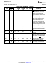
Read Enable. Active-low read strobe. The
read strobe waveform is specified, per zone
basis, by the Lead, Active, and Trail periods
XRD 41 48 4900.6 42.6 O/Z –
in the XTIMINGx registers.
NOTE: The XRD and XWE signals are
mutually exclusive.
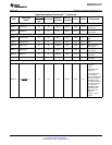
Read Not Write Strobe. Normally held high.
When low, XR/W indicates write cycle is
XR/W 50 57 5361.5 755.0 O/Z –
active; when high, XR/W indicates read
cycle is active.
Ready Signal. Indicates peripheral is ready
to complete the access when asserted to 1.
XREADY 157 176 42.6 1972.4 I PU XREADY can be configured to be a
synchronous or an asynchronous input.
See the timing diagrams for more details.
18 Introduction Copyright © 2009–2010, Texas Instruments Incorporated
Submit Documentation Feedback
Product Folder Link(s): SM320F2812-HT