


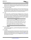
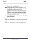
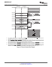
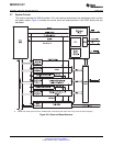

XD(15:0)
XA(18:0)
XZCS6
XZCS7
XZCS6AND7
XZCS2
XWE
XR/W
XREADY
XMP/MC
XHOLD
XHOLDA
XCLKOUT
XRD
XINTF Zone 0
(8K × 16)
XINTF Zone 1
(8K × 16)
XINTF Zone 6
(512K × 16)
XINTF Zone 7
(16K × 16)
(mapped here if MP/MC
= 1)
0x40 0000
0x3F C000
0x18 0000
0x10 0000
0x00 6000
0x00 4000
0x00 2000
0x00 0000
Data Space Prog Space
XINTF Zone 2
(512K × 16)
0x08 0000
XZCS0AND1
XZCS0
XZCS1
SM320F2812-HT
SGUS062A–JUNE 2009–REVISED APRIL 2010
www.ti.com
A. The mapping of XINTF Zone 7 is dependent on the XMP/MC device input signal and the MP/MC mode bit (bit 8 of
XINTCNF2 register). Zones 0, 1, 2, and 6 are always enabled.
B. Each zone can be programmed with different wait states, setup and hold timing, and is supported by zone chip
selects (XZCS0AND1, XZCS2, XZCS6AND7), which toggle when an access to a particular zone is performed. These
features enable glueless connection to many external memories and peripherals.
C. The chip selects for Zone 0 and 1 are ANDed internally together to form one chip select (XZCS0AND1). Any external
memory that is connected to XZCS0AND1 is dually mapped to both Zones 0 and Zone 1.
D. The chip selects for Zone 6 and 7 are ANDed internally together to form one chip select (XZCS6AND7). Any external
memory that is connected to XZCS6AND7 is dually mapped to both Zones 6 and Zone 7. This means that if Zone 7 is
disabled (via the MP/MC mode) then any external memory is still accessible via Zone 6 address space.
Figure 3-3. External Interface Block Diagram
40 Functional Overview Copyright © 2009–2010, Texas Instruments Incorporated
Submit Documentation Feedback
Product Folder Link(s): SM320F2812-HT