


SM320F2812-HT
www.ti.com
SGUS062A–JUNE 2009–REVISED APRIL 2010
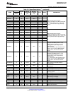
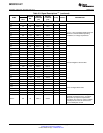
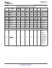
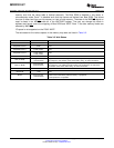
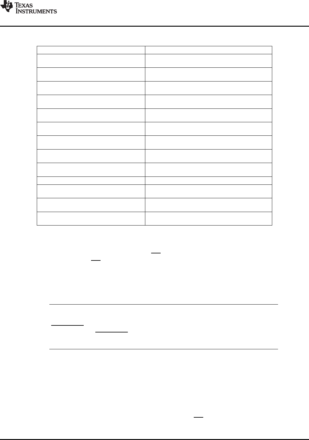
Table 3-1. Addresses of Flash Sectors in F2812
ADDRESS RANGE PROGRAM AND DATA SPACE
0x3D 8000
Sector J, 8K × 16
0x3D 9FFF
0x3D A000
Sector I, 8K × 16
0x3D BFFF
0x3D C000
Sector H, 16K × 16
0x3D FFFF
0x3E 0000
Sector G, 16K × 16
0x3E 3FFF
0x3E 4000
Sector F, 16K × 16
0x3E 7FFF
0x3E 8000
Sector E, 16K × 16
0x3E BFFF
0x3E C000
Sector D, 16K × 16
0x3E FFFF
0x3F 0000
Sector C, 16K × 16
0x3F 3FFF
0x3F 4000
Sector B, 8K × 16
0x3F 5FFF
0x3F 6000 Sector A, 8K × 16
0x3F 7F80 Program to 0x0000 when using the
0x3F 7FF5 Code Security Module
0x3F 7FF6 Boot-to-Flash (or ROM) Entry Point
0x3F 7FF7 (program branch instruction here)
0x3F 7FF8 Security Password (128-Bit)
0x3F 7FFF (Do not program to all zeros)
The Low 64K of the memory address range maps into the data space of the 240x. The High 64K of the
memory address range maps into the program space of the 24x/240x. 24x/240x-compatible code only
executes from the High 64K memory area. Hence, the top 32K of Flash/ROM and H0 SARAM block can
be used to run 24x/240x-compatible code (if MP/MC mode is low) or, on the F2812, code can be executed
from XINTF Zone 7 (if MP/MC mode is high).
The XINTF consists of five independent zones. One zone has its own chip select and the remaining four
zones share two chip selects. Each zone can be programmed with its own timing (wait states) and to
either sample or ignore external ready signal. This makes interfacing to external peripherals easy and
glueless.
NOTE
The chip selects of XINTF Zone 0 and Zone 1 are merged together into a single chip select
(XZCS0AND1); and the chip selects of XINTF Zone 6 and Zone 7 are merged together into a
single chip select (XZCS6AND7). See Section 3.5, External Interface, XINTF (2812 only), for
details.
Peripheral Frame 1, Peripheral Frame 2, and XINTF Zone 1 are grouped together so as to enable these
blocks to be write/read peripheral block protected. The protected mode ensures that all accesses to these
blocks happen as written. Because of the C28x pipeline, a write immediately followed by a read, to
different memory locations, appears in reverse order on the memory bus of the CPU. This can cause
problems in certain peripheral applications where the user expected the write to occur first (as written).
The C28x CPU supports a block protection mode where a region of memory can be protected so as to
make sure that operations occur as written (the penalty is extra cycles are added to align the operations).
This mode is programmable and by default, it protects the selected zones.
On the F2812, at reset, XINTF Zone 7 is accessed if the XMP/MC pin is pulled high. This signal selects
microprocessor or microcomputer mode of operation. In microprocessor mode, Zone 7 is mapped to high
Copyright © 2009–2010, Texas Instruments Incorporated Functional Overview 29
Submit Documentation Feedback
Product Folder Link(s): SM320F2812-HT