


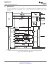

X2
X1/XCLKIN
On-Chip
Oscillator
(OSC)
PLL
Bypass
/2
XF_XPLLDIS
OSCCLK (PLL Disabled)
Latch
XPLLDIS
XRS
PLL
4-Bit PLL Select
SYSCLKOUT
1
0
CLKIN
CPU
4-Bit PLL Select
XCLKIN
PLL Block
SM320F2812-HT
SGUS062A–JUNE 2009–REVISED APRIL 2010
www.ti.com
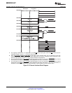
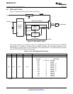
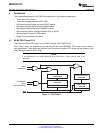
3.8 OSC and PLL Block
Figure 3-7 shows the OSC and PLL block on the F2812.
Figure 3-7. OSC and PLL Block
The on-chip oscillator circuit enables a crystal to be attached to the F2812 device using the X1/XCLKIN
and X2 pins. If a crystal is not used, then an external oscillator can be directly connected to the
X1/XCLKIN pin and the X2 pin is left unconnected. The logic-high level in this case should not exceed
V
DD
. The PLLCR bits [3:0] set the clocking ratio.
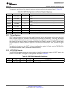
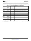
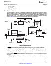
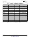
Table 3-14. PLLCR Register Bit Definitions
BIT(S) NAME TYPE XRS RESET
(1)
DESCRIPTION
15:04 reserved R = 0 0:00
SYSCLKOUT = (XCLKIN x n)/2, where n is the PLL multiplication factor.
Bit Value n SYSCLKOUT
0000 PLL Bypassed XCLKIN/2
0001 1 XCLKIN/2
0010 2 XCLKIN
0011 3 XCLKIN × 1.5
0100 4 XCLKIN × 2
0101 5 XCLKIN × 2.5
0110 6 XCLKIN × 3
3:00 DIV R/W 0,0,0,0
0111 7 XCLKIN × 3.5
1000 8 XCLKIN × 4
1001 9 XCLKIN × 4.5
1010 10 XCLKIN × 5
1011 11 Reserved
1100 12 Reserved
1101 13 Reserved
1110 14 Reserved
1111 15 Reserved
(1) The PLLCR register is reset to a known state by the XRS reset line. If a reset is issued by the debugger, the PLL clocking ratio is not
changed.
48 Functional Overview Copyright © 2009–2010, Texas Instruments Incorporated
Submit Documentation Feedback
Product Folder Link(s): SM320F2812-HT