


SM320F2812-HT
SGUS062A–JUNE 2009–REVISED APRIL 2010
www.ti.com
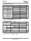
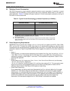
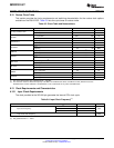
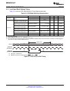
6.12 Device Clock Table
This section provides the timing requirements and switching characteristics for the various clock options
available on the F2812 DSP. Table 6-3 lists the cycle times of various clocks.
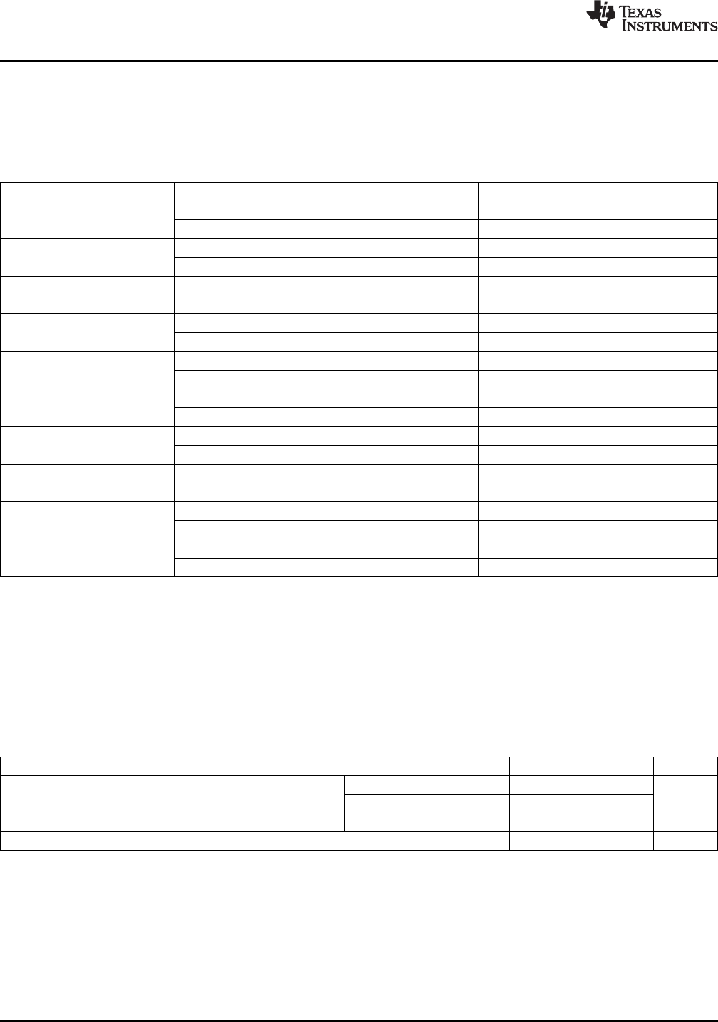
Table 6-3. Clock Table and Nomenclature
MIN NOM MAX UNIT
t
c(OSC)
, Cycle time 28.6 50 ns
On-chip oscillator clock
Frequency 20 35 MHz
t
c(CI)
, Cycle time 6.67 250 ns
XCLKIN
Frequency 4 150 MHz
t
c(SCO)
, Cycle time 6.67 500 ns
SYSCLKOUT
Frequency 2 150 MHz
t
c(XCO)
, Cycle time 6.67 2000 ns
XCLKOUT
Frequency 0.5 150 MHz
t
c(HCO)
, Cycle time 6.67 13.3
(1)
ns
HSPCLK
Frequency 75
(1)
150 MHz
t
c(LCO)
, Cycle time 13.3 26.6
(1)
ns
LSPCLK
Frequency 37.5
(1)
75 MHz
t
c(ADCCLK)
, Cycle time
(2)
40 ns
ADC clock
Frequency 25 MHz
t
c(SPC)
, Cycle time 50 ns
SPI clock
Frequency 20 MHz
t
c(CKG)
, Cycle time 50 ns
McBSP
Frequency 20 MHz
t
c(XTIM)
, Cycle time 6.67 ns
XTIMCLK
Frequency 150 MHz
(1) This is the default reset value if SYSCLKOUT = 150 MHz.
(2) The maximum value for ADCCLK frequency is 25 MHz. For SYSCLKOUT values of 25 MHz or lower, ADCCLK has to be
SYSCLKOUT/2 or lower. ADCCLK = SYSCLKOUT is not a valid mode for any value of SYSCLKOUT.
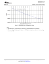
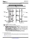
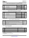
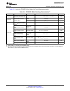
6.13 Clock Requirements and Characteristics
6.13.1 Input Clock Requirements
The clock provided at the XCLKIN pin generates the internal CPU clock cycle.
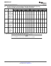
Table 6-4. Input Clock Frequency
(1)
PARAMETER MIN TYP MAX UNIT
Resonator
(2)
20 35
f
x
Input clock frequency Crystal
(2)
20 35 MHz
XCLKIN 4 150
f
l
Limp mode clock frequency 2 MHz
(1) Not production tested.
(2) Not guaranteed for T
A
> 125°C.
94 Electrical Specifications Copyright © 2009–2010, Texas Instruments Incorporated
Submit Documentation Feedback
Product Folder Link(s): SM320F2812-HT