


SM320F2812-HT
www.ti.com
SGUS062A–JUNE 2009–REVISED APRIL 2010
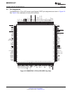
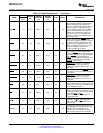
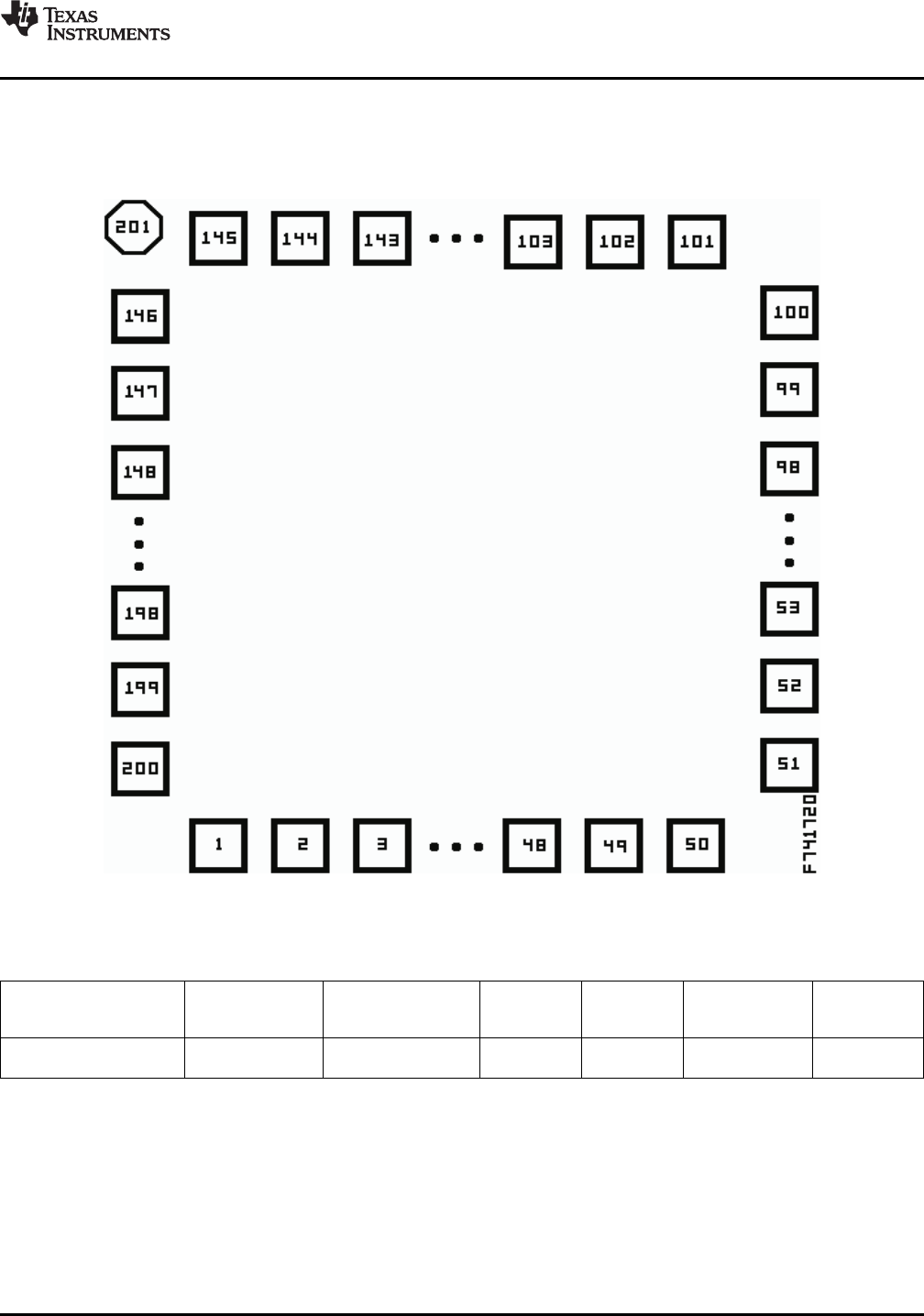
2.3 Die Layout
The SM320F2812 die layout is shown in Figure 2-1. See Table 2-3 for a description of each pad's
function.
Figure 2-1. SM320F2812 Die Layout
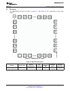
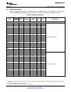
Table 2-2. Bare Die Information
DIE PAD
DIE PAD DIE BACKSIDE BACKSIDE
DIE SIZE DIE PAD SIZE COMPOSITI
COORDINATES THICKNESS FINISH POTENTIAL
ON
219.4 x 207.0 (mils); Silicon with
55.0 x 64.0 (mm) See Table 2-3 11.0 mils AlCu/TiN Ground
5572.0 x 5258.0 (mm) backgrind
Copyright © 2009–2010, Texas Instruments Incorporated Introduction 15
Submit Documentation Feedback
Product Folder Link(s): SM320F2812-HT