


TNETX4090
ThunderSWITCH II
9-PORT 100-/1000-MBIT/S ETHERNET
SWITCH
SPWS044E – DECEMBER 1997 – REVISED AUGUST 1999
15
POST OFFICE BOX 655303 • DALLAS, TEXAS 75265
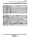
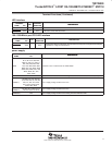
Terminal Functions (Continued)
RDRAM interface
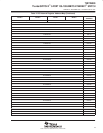
TERMINAL
I/O
INTERNAL
DESCRIPTION
NAME NO.
I/O
RESISTOR
DESCRIPTION
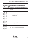
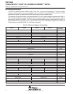
DBUS_CTL
Y26 O None
Bus control. Controls signal-to-frame packets, transmits part of the operation code,
initiates data transfers, and terminates data transfers. This is a rambus signal logic (RSL)
signal (see Note 1).
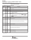
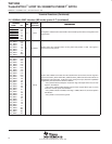
DBUS_DATA0
DBUS_DATA1
DBUS_DATA2
DBUS_DATA3
DBUS_DATA4
DBUS_DATA5
DBUS_DATA6
DBUS_DATA7
DBUS_DATA8
AC26
AA24
AB26
Y24
V24
U25
U26
T26
R25
I/O None
Bus data. Signal lines for request, write-data, and read-data packets. The request packet
contains the address, operation codes, and other control information. These are RSL
signals (see Note 1).
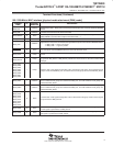
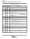
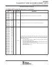
DBUS_EN
T25 O None
Bus enable. Controls signal-to-transfer column addresses for random-access
(nonsequential) transactions. This is an RSL signal (see Note 1).
DCCTRL
P24 I None
Current control program. Connected to the current control resistor whose other terminal
is connected to the termination voltage.
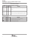
DRX_CLK
V26 O None
Receive clock. This signal is derived from DTX_CLK. This is an RSL signal (see Note 1).
It is connected directly to DTX_CLK in the TNETX4090.
DTX_CLK
V25 I None
Transmit clock. This is an RSL signal (see Note 1). The primary internal clock is derived
from this signal.
DVREF
AA26 I None Reference voltage. Logic threshold reference voltage for RSL signals.
NOTE 1: RSL is a low-voltage swing, active-low signaling technology.