


TNETX4090
ThunderSWITCH II
9-PORT 100-/1000-MBIT/S ETHERNET
SWITCH
SPWS044E – DECEMBER 1997 – REVISED AUGUST 1999
61
POST OFFICE BOX 655303 • DALLAS, TEXAS 75265
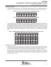
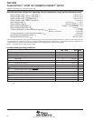
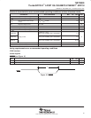
electrical characteristics over recommended operating conditions (unless otherwise noted)
PARAMETER TEST CONDITIONS MIN TYP MAX UNIT
V
OH
High-level output voltage I
OH
= rated V
DD(3.3)
–0.5 V
V
OL
Low-level output voltage I
OL
= rated 0.5 V
I
OZ
High-impedance-state output
current
V
O
= V
DD
or GND ±10 µA
I
IH
High-level input current V
I
= V
IH
1 µA
I
IL
Low-level input current V
I
= V
IL
–1 µA
V
OHR
High-level output voltage (RSL) I
OH
2 V
DD
V
V
OLR
Low-level output voltage (RSL) 0 0.4 V
I
DD(2.5V)
V
DD(2.5V)
= max,
DTX_CLK and DRX_CLKf = 83.33 MHz
1.5
I
DD(3.3V)
Supply current
V
DD(3.3V)
= max,
DTX_CLK and DRX_CLKf = 83.33 MHz
0.5
A
I
DD(2.5)
V
DD(2.5)
= max,
DTX_CLK and DRX_CLKf = 83.33 MHz
0.175
C
i
Capacitance, input 6 pF
C
o
Capacitance, output 6 pF
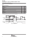
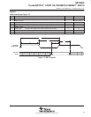
timing requirements over recommended operating conditions
JTAG interface
control signals
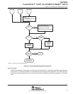
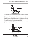
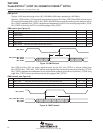
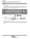
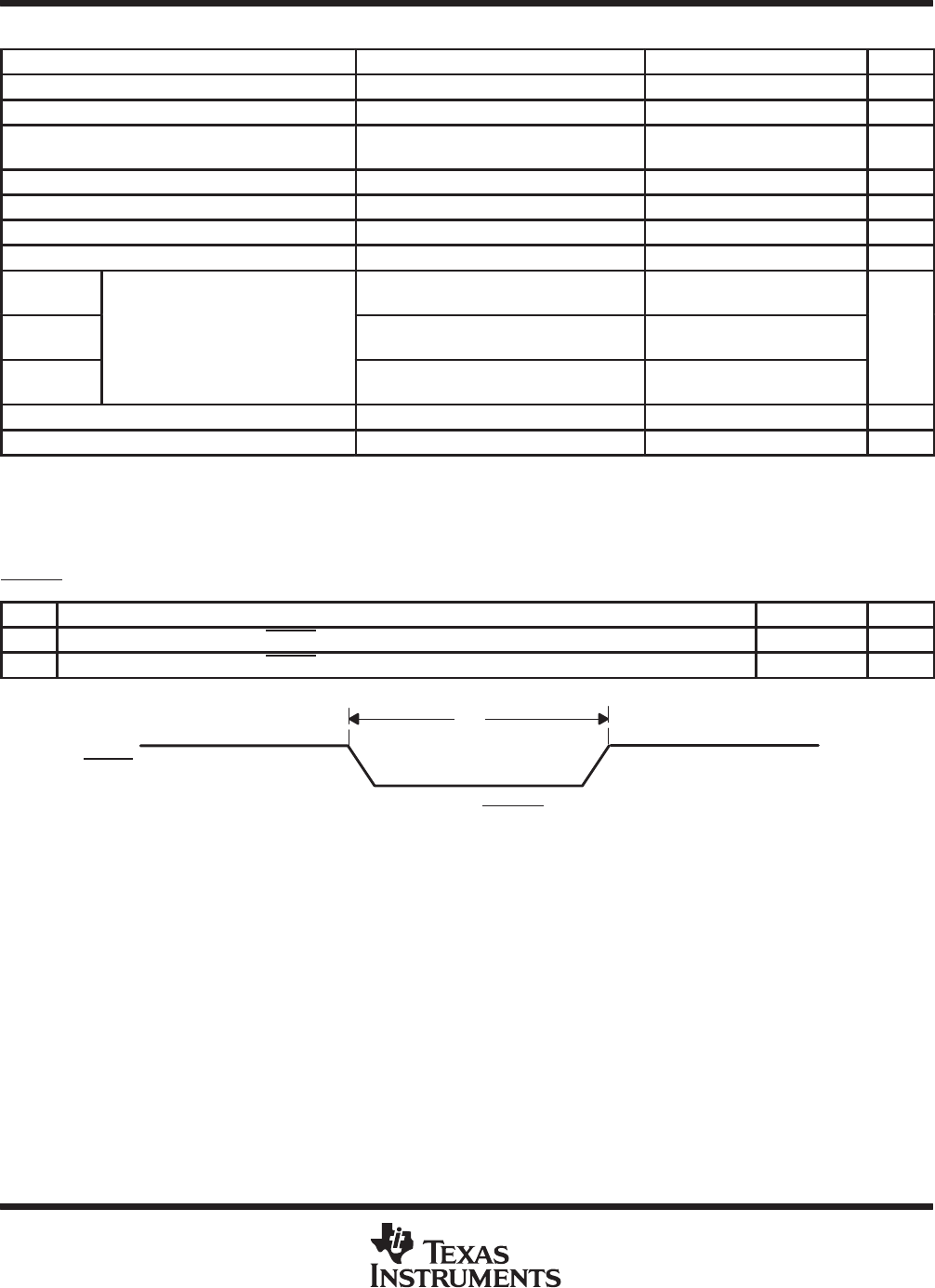
RESET (see Figure 15)
NO. MIN MAX UNIT
1 t
w(RESETP)
Pulse duration, RESET low at power up 100 µs
1 t
w(RESET)
Pulse duration, RESET low at other times 4 t
cycle
1
RESET
Figure 15. RESET