TMP92CM22
2007-02-16
92CM22-135
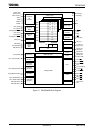
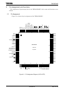
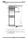
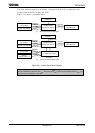
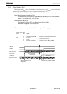
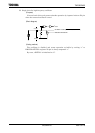
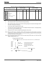
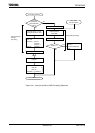
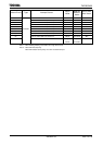
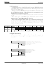
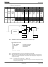
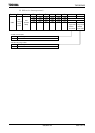
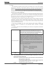
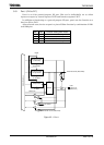
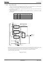
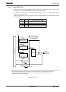
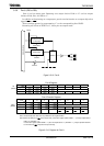
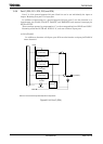
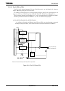
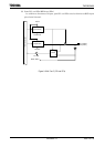
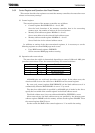
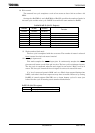
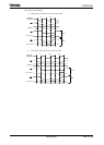
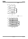
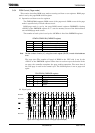
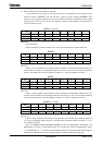
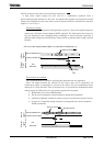
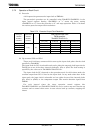
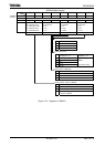
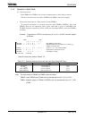
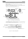
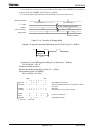
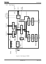
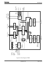
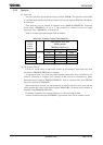
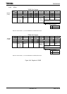
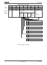
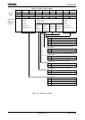
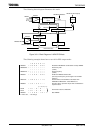
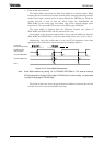
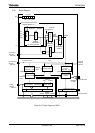
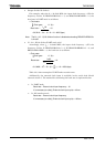
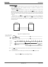
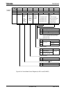
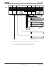
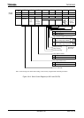
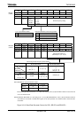
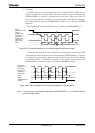
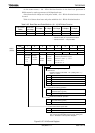
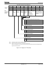
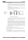
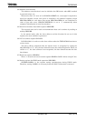
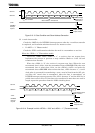
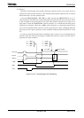
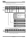
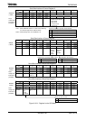
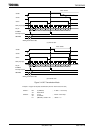
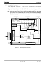
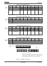
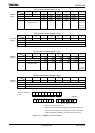
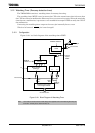
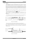
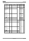
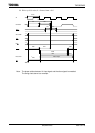
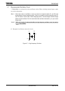
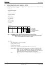
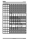
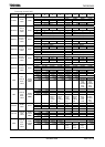
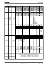
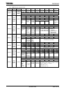
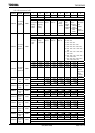
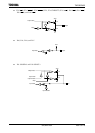
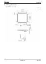
The following block diagram illustrates this mode.
Figure 3.8.11 Block Diagram of 16-Bit PPG Mode
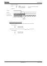
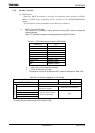
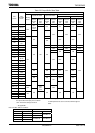
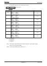
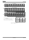
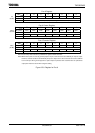
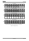
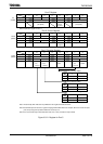
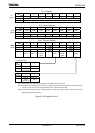
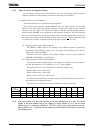
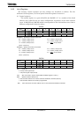
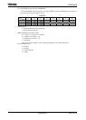
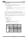
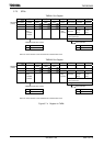
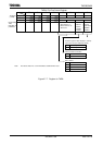
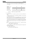
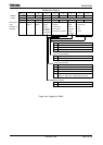
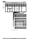
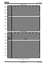
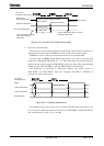
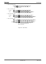
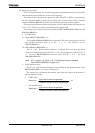
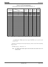
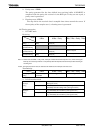
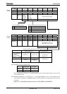
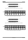
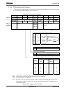
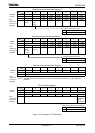
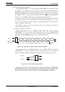
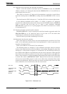
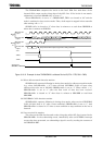
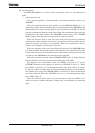
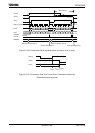
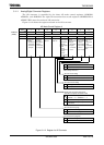
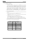
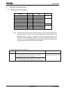
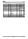
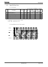
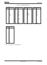
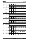
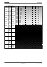
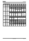
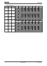
The following example shows how to set 16-bit PPG output mode:
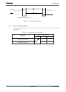
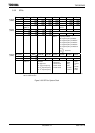
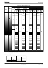
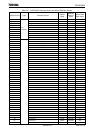
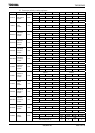
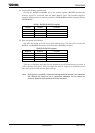
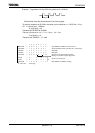
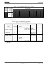
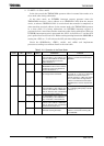
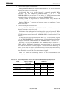
7 6 5 4 3210
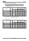
TB0RUN ← 0 0 X X −
0 X 0 Disable the TB0RG0H/L double buffer and stop TMRB0.
TB0RG0H/L ← * * * * * * * * Set the duty ratio.
* * * * * * * * (16 bits)
TB0RG1H/L ← * * * * * * * * Set the frequency.
* * * * * * * * (16 bits)
TB0RUN ← 1 0 X X −
0 X 0 Enable the TB0RG0 double buffer.
(The duty and frequency are changed on an INTTB01
interrupt.)
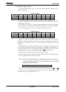
TB0FFCR ← X X 0 0 1110 Set the mode to invert TB0FF0 at the match with
TB0RG0H/L/TB0RG1H?L. Clear TB0FF0 to 0.
TB0MOD ← 0 0 1 0 0 1 ** Set input clock to prescaler output clock and disable the
capture function.
(** = 01, 10, 11)
PCCR ← X 1 − X −
X −
−
PCFC ← X 1 − X −
X −
−
Set PC6 to function as TB0OUT0.
TB0RUN ← 1 0 X X −
1X1 Start TMRB0.
X : Don’t care, − : No change
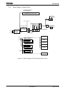
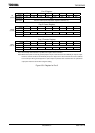
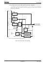
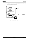
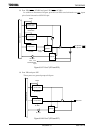
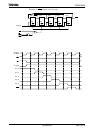
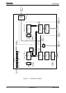
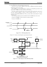
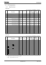
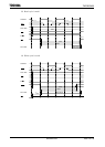
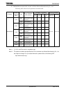
16-bit up counter
UC10
16-bit comparator 16-bit comparator
TB0IN0
φT1
φT4
φT16
F/F
(TB0FF0)
TB0RG0H/L
Register buffer 10 TB0REG1H/L
TB0RUN<TB0RDE>
TB0RG0-WR
TB0RUN<TB0RUN>
TB0OUT0 (PPG output)
Internal data bus
Selecto
Matching
Selecto
Clear