TMP92CM22
2007-02-16
92CM22-53
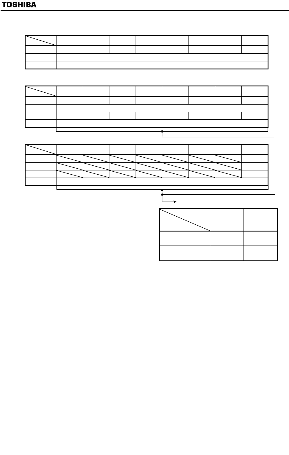
Port 1 Register
7 6 5 4 3 2 1 0
Bit symbol P17 P16 P15 P14 P13 P12 P11 P10
Read/Write R/W
After reset Data from external port (Output latch register is clear to “0”.)
Port 1 Control Register
7 6 5 4 3 2 1 0
Bit symbol P17C P16C P15C P14C P13C P12C P11C P10C
Read/Write W
After reset 0 0 0 0 0 0 0 0
Function Refer to port 1 function setting
Port 1 Function Register
7 6 5 4 3 2 1 0
Bit symbol P1F
Read/Write W
After reset 0/1 Note3
Function Refer to port 1 function setting
Port 1 Function setting
Note 1: Read-modify-write instruction is prohibited for registers
P1FC and P1CR.
Note 2: <P1XC> shows “X bit” of P1CR register.
Note 3: It is set to “Port” or “Data bus” by AM pin setting.
Figure 3.5.2 Register for Port 1
P1
(0004H)
P1CR
(0006H)
P1FC
(0007H)
P1FC<P1F>
P1CR<P1xC>
0 1
0 Input port
Data bus
(D15 to D8)
1 Output port
Don’t use this
setting


