Virtex-5 FPGA ML561 User Guide www.xilinx.com 135
UG199 (v1.2) April 19, 2008
Hardware Schematic Diagram
R
LCD Panel Used in Character Mode
This design example requires a byte representing a command or data to be displayed as
input.
• When the Enable signal is Low, nothing happens. The display interface design is
locked.
• When the Enable signal is High and the data_or_command control signal is Low, the
byte written is a display command.
• When the Enable signal and the data_or_command control signal are High, the byte
written is the ASCII character code of the character to be put on the display.
Display Command Byte
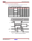
The command set of the display can be found in Table C-6, page 130.
When the LCD interface is enabled for the first time, a set of command bytes is sent to the
LCD. This command set provides the basic initialization of the LCD controller. When this
initialization is done, the normal LCD interface is freed for normal use. Command bytes
from the valid command set can be sent to the display (controller).
The Toplevel.vhd.txt file provides a detailed description of the LCD controller
interface.
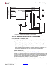
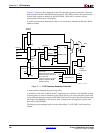
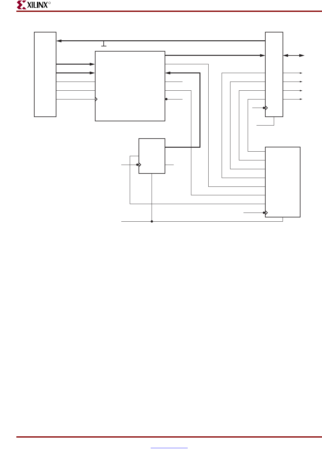
Figure C-8: General Block Diagram of LCD Panel in Full Graphics Mode
UG199_C_08_050106
Block RAM
IorD = '1' Instruction
'0' Data
Design for Full Graphics Interface, Attached to CoreConnect Bus
Enable
Write
Address
WData (32+4)
RData (8+gnd)
ena
Clock
read
Addr
IorD (bit 9)
DataIn (8)
DataOut (8)
RW
E
Clock
Reset
Clock
Reset
Clock
E
TC
RS
CS1B
DB (8)
CoreConnect
State
Machine
Clock


