Virtex-5 FPGA ML561 User Guide www.xilinx.com 37
UG199 (v1.2) April 19, 2008
Board Design Considerations
R
For Write data and terminations at the memory, if the trace length from the receiver pin to
the termination resistor can be guaranteed to be within 0.3 inches, then the fly-by
termination scheme is implemented. Otherwise, the non-fly-by termination topology is
implemented for Write data at the memory end.
The physical dimensions of the raw PCB are 12.75 inches x 11.75 inches. With the
overhangs due to edge connectors, the actual size of the fully assembled board is
approximately 13 inches x 12 inches, with 1.5 inches height allowance for the DIMM
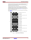
modules. This 14-layer board has 6 signal layers, 4 GND layers, and 4 power planes and
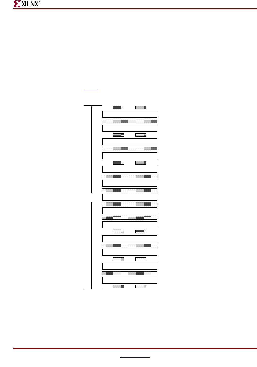
uses Polyclad 370HR material for lead-free assembly. Figure 3-11 shows a stack-up
diagram of the ML561 Revision A PCB.
Refer to UG203
, Virtex-5 PCB Designer’s Guide for more information on the PCB design
using Virtex-5 devices.
Figure 3-11: ML561 Revision A PCB Stack-Up
73.90 ±7 mils
UG199_c3_11_102407
1.0 oz, TOP, Z
0
= 50Ω, width = 6 mils
3.8 mils, Er = 4.4
1.0 oz, 02_GND1
4 mils, Er = 4.4
0.5 oz, 03_INR1, Z
0
= 50Ω, width = 4.5 mils
5.3 mils, Er = 4.4
1.0 oz, 04_PWR1
8 mils, Er = 4.4
0.5 oz, 05_INR2, Z
0
= 50Ω, width = 4.5 mils
3.2 mils, Er = 4.4
1.0 oz, 06_GND2
3 mils, Er = 4.4
1.0 oz, 07_PWR2
3.3 mils, Er = 4.4
1.0 oz, 08_PWR3
3 mils, Er = 4.4
1.0 oz, 09_GND3
3.2 mils, Er = 4.4
0.5 oz, 10_INR5, Z
0
= 50Ω, width = 4.5 mils
8 mils, Er = 4.4
1.0 oz, 11_PWR4
5.3 mils, Er = 4.4
0.5 oz, 12_INR6, Z
0
= 50Ω, width = 4.5 mils
4 mils, Er = 4.4
1.0 oz, 13_GND4
3.8 mils, Er = 4.4
1.0 oz, BOTTOM, Z
0
= 50Ω, width = 6 mils


