Virtex-5 FPGA ML561 User Guide www.xilinx.com 9
UG199 (v1.2) April 19, 2008
Conventions
R
Conventions
This document uses the following conventions. An example illustrates each convention.
Typographical
This document uses the following typographical conventions. An example illustrates each
convention.
Online Document
The following conventions are used in this document:
Terminology
This section defines terms used in Chapter 7, “ML561 Hardware-Simulation Correlation,”
of this document.
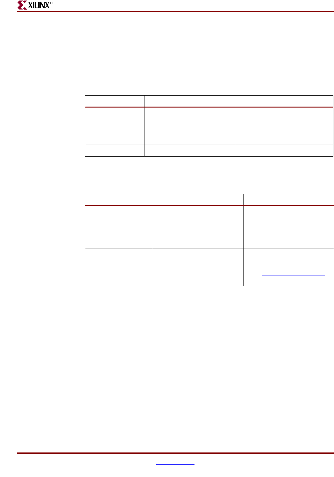
Convention Meaning or Use Example
Italic font
References to other documents
See the Virtex-5 Configuration Guide
for more information.
Emphasis in text
The address (F) is asserted after
clock event 2.
Underlined Text
Indicates a link to a web page. http://www.xilinx.com/virtex5
Convention Meaning or Use Example
Blue text
Cross-reference link to a location
in the current document
See the section “Additional
Documentation” for details.
Refer to “Clock Management
Technology (CMT)” in
Chapter 2 for details.
Red text
Cross-reference link to a location
in another document
See Figure 5 in the Virtex-5 FPGA
Data Sheet
Blue, underlined text
Hyperlink to a website (URL)
Go to http://www.xilinx.com
for the latest documentation.
Data Valid Window (DVW)
DVW is the data valid window opening measured by the VIH and VIL masks. The
smaller of the two values are listed as absolute time as well as in terms of the percentage
of UI (Unit Interval), or bit time.
Extrapolation
The ultimate goal of a design is to ascertain quality of signal at the receiver I/O Buffer
(IOB). This measurement can only be simulated. When the hardware measurements are
correlated with the simulation at the probe point, the extra probe capacitance is
removed from the IBIS schematics, and the simulation is repeated at two extreme
corners (slow-weak and fast-strong). Removal of probe capacitance is important to
represent the actual hardware. If the SI characteristics of these simulations are proved
to be within the acceptable range with sufficient margin, then the performance
requirements for data signal interface of the corresponding memory operation at the
target clock frequency are proved to have been met.


