16 www.xilinx.com Virtex-5 FPGA ML561 User Guide
UG199 (v1.2) April 19, 2008
Chapter 2: Getting Started
R
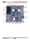
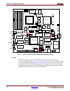
5. Insert the CompactFlash card included in the kit into socket J27 on the Virtex-5 FPGA
ML561 Development Board. To select the startup file, check that SW8 is set to position
0.
Applying Power to the Board
The Virtex-5 FPGA ML561 Development Board is now ready to power on. The Virtex-5
FPGA ML561 Development Board is shipped with a country-specific AC line cord for the
universal input 5V desktop power supply. Follow these steps to power up the Virtex-5
FPGA ML561 Development Board:
1. Confirm that the ON-OFF switch, SW5, is in the OFF position.
2. Plug the 5V desktop power supply into the 5V DC input barrel jack J28 on the Virtex-5
FPGA ML561 Development Board. Plug the desktop power supply AC line cord into
an electrical outlet supplying the appropriate voltage.
3. Turn SW5 to the ON position. The power indicators for all regulator modules should
come on, indicating output from the regulators. The System ACE status LED D37
comes on when the System ACE controller (U45) extracts the BIT configuration file
from the CompactFlash card to the FPGA. If no CompactFlash card is installed in the
card socket J27 on the Virtex-5 FPGA ML561 Development Board, the red System ACE
error LED D38 flashes.
4. If a CompactFlash card is not installed in socket J27, a JTAG cable must be used to
configure the FPGAs. To use a Parallel IV cable or other JTAG pod, download the
FPGA configuration bitstream into each FPGA. After the DONE LED (D28) comes on,
the FPGAs are configured and ready to use.
5. Push the reset button SW4.


