138 www.xilinx.com Virtex-5 FPGA ML561 User Guide
UG199 (v1.2) April 19, 2008
Appendix C: LCD Interface
R
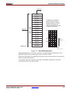
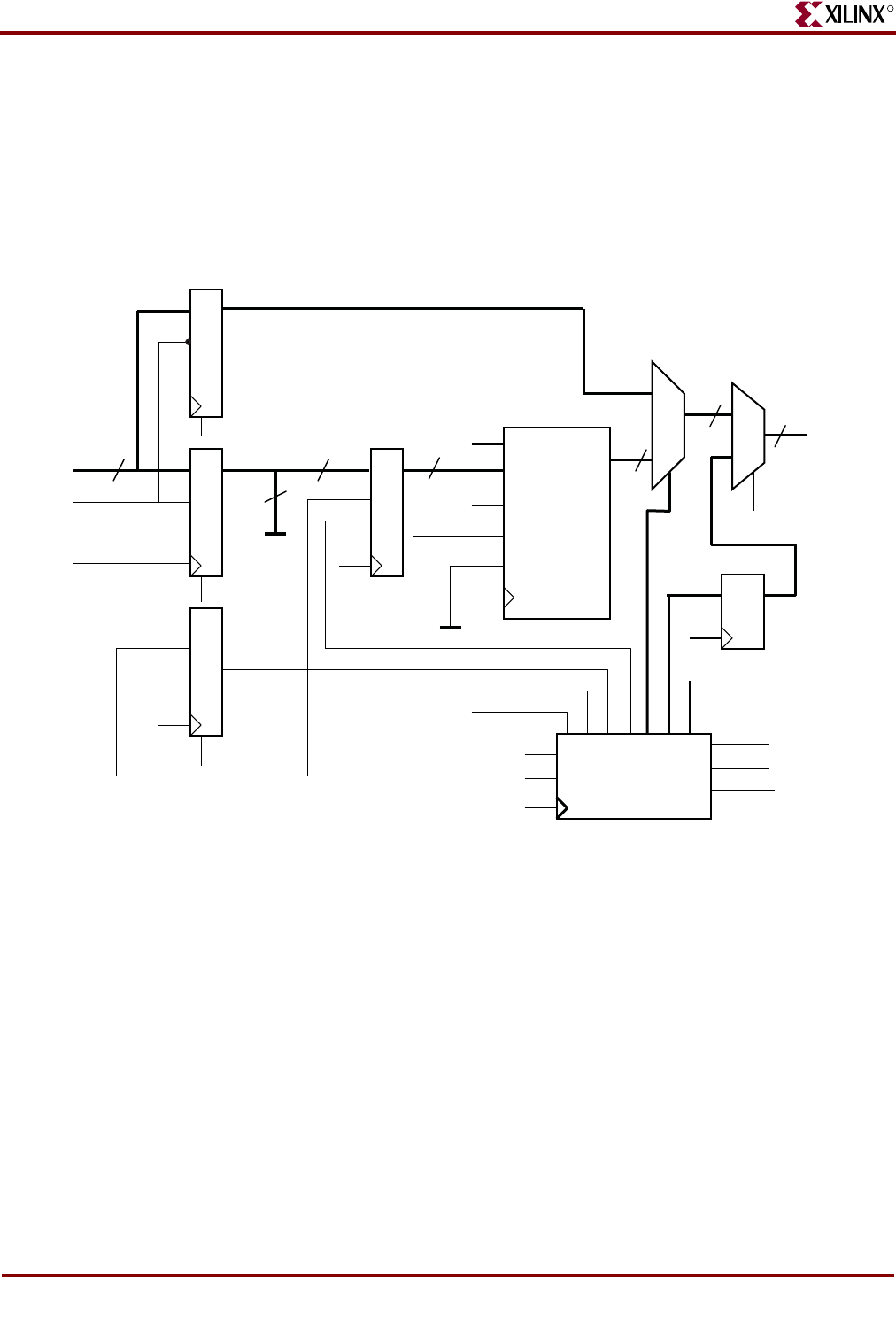
Figure C-11 shows a block diagram of the LCD character generator controller. Character
data is latched and then shifted left three positions. This shifted value is the start byte for a
counter that outputs an address to the block RAM. The result is a stream of bytes
representing a character for the display.
A small second counter determines when a new character is loaded into the block RAM
address counter.
A state machine manages the processing order.
A minimum cycle time of 400 ns on the E signal used as a reference. The 200 MHz system
clock frequency is used as reference system clock. One E cycle uses at least 80 system clock
cycles when the design is running at 200 MHz. The E pulse is part of the state machine, and
the design only depends on the system clock. Timing is met as long as the system clock
does not exceed 200 MHz.
This design can be adapted easily to fit the MicroBlaze™ or PPC405 CoreConnect bus
system.
Figure C-11: LCD Character Generator Controller
TC
L
Addr
DI
E E
RAMB16_S9
Counter B
Counter A
Position
Register
Clk
Ena
DataIn
Ena
E
Load
Clk
Clk
Clk
We
DO
Ssr
8
3
11
11
8
Count to 8.
Stop both counters at TC.
Send character position and
line to the LCD.
Load new va lue in counter A.
Switch to character ROM.
Enable counters.
8
Clk
Ena
State Machine
Page
Rst
Rst
Display
Register
DesRst
DesRst DesRst
DesRst
DesRst
DesRst
8
Clk
LUT-ROM
Display
Initialization
RS
RW
Data
E
1
0
UG199_C_11_050106


