Virtex-5 FPGA ML561 User Guide www.xilinx.com 7
UG199 (v1.2) April 19, 2008
R
Preface
About This Guide
This user guide describes the Virtex
®
-5 FPGA ML561 Memory Interfaces Development
Board. Complete and up-to-date documentation of the Virtex-5 family of FPGAs is
available on the Xilinx website at http://www.xilinx.com/virtex5
.
Guide Contents
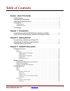
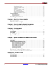
This manual contains the following chapters:
• Chapter 1, “Introduction”
• Chapter 2, “Getting Started”
• Chapter 3, “Hardware Description”
• Chapter 4, “Electrical Requirements”
• Chapter 5, “Signal Integrity Recommendations”
• Chapter 6, “Configuration”
• Chapter 7, “ML561 Hardware-Simulation Correlation”
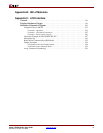
• Appendix A, “FPGA Pinouts”
• Appendix B, “Bill of Materials”
• Appendix C, “LCD Interface”
Additional Documentation
The following documents are also available for download at
http://www.xilinx.com/virtex5
.
• Virtex-5 Family Overview
The features and product selection of the Virtex-5 family are outlined in this overview.
• Virtex-5 FPGA Data Sheet: DC and Switching Characteristics
This data sheet contains the DC and Switching Characteristic specifications for the
Virtex-5 family.
• Virtex-5 FPGA User Guide
Chapters in this guide cover the following topics:
- Clocking Resources
- Clock Management Technology (CMT)
- Phase-Locked Loops (PLLs)
-Block RAM


