Virtex-5 FPGA ML561 User Guide www.xilinx.com 39
UG199 (v1.2) April 19, 2008
R
Chapter 4
Electrical Requirements
This chapter provides the electrical requirements for the Virtex-5 FPGA ML561
Development Board. It contains the following sections:
• “Power Consumption”
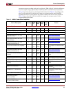
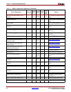
• “FPGA Internal Power Budget”
Power Consumption
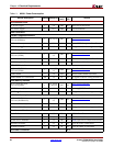
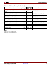
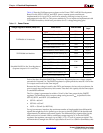
Table 4-1 lists the operating voltages, maximum currents, and power consumption used by
the ML561 board devices. The Virtex-5 FPGA ML561 Development Board has provisions
for two power inputs: a 5V power supply and a 12V power supply. The maximum rating of
a commercially available 5V power supply is limited to 8A, or a 40W maximum capacity.
This power supply is similar to the 5V brick used for previous memory tool kits, for
example, ML461. This tool kit expects the Virtex-5 FPGA ML561 Development Board to
exercise only one external memory interface at a time. In this case, the total power
consumption of the board stays within the 40W limit.
As shown in Table 4-1, if all three FPGA devices and their associated memory devices are
activated simultaneously, then the total power consumption is approximately 57W, which
exceeds the 40W capacity of the 5V power brick. So an alternate 12V power input jack (J23)
is provided on the Virtex-5 FPGA ML561 Development Board to hook up a 12V power
brick, for example, CUI DTS120500U with a 60W capacity. The 12V is converted to 5V
using the TI PTH12010WAS power module (VR11), which can supply up to 12A of current
at 5V, or a 60W capacity.


