Virtex-5 FPGA ML561 User Guide www.xilinx.com 17
UG199 (v1.2) April 19, 2008
R
Chapter 3
Hardware Description
This chapter describes the major hardware blocks on the Virtex-5 FPGA ML561
Development Board and provides useful design consideration. It contains the following
sections:
• “Hardware Overview”
• “Memory Details”
• “External Interfaces”
• “Power Regulation”
• “Board Design Considerations”
Hardware Overview
The ML561 Development/Evaluation system reference design is implemented with three
XC5VLX50T-FFG1136 devices from the Virtex-5 FPGA family to demonstrate high-speed
external memory application interfaces. The memory technologies supported by the
Virtex-5 FPGA ML561 Development Board are DDR2 SDRAM, DDR400 SDRAM, QDRII
SRAM, and RLDRAM II SDRAM.
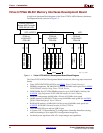
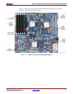
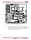
Figure 3-1 provides a view of all the major components on ML561 board. It shows the
placement of the three Virtex-5 FPGAs, and the position of the associated major interfaces
for each FPGA.


