52 www.xilinx.com Virtex-5 FPGA ML561 User Guide
UG199 (v1.2) April 19, 2008
Chapter 6: Configuration
R
JTAG Chain
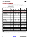
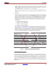
Four devices (the System ACE chip and three XC5VLX50T-FFG1136 FPGAs) are connected
via a JTAG chain on the Virtex-5 FPGA ML561 Development Board. The order of the four
devices in the JTAG chain is System ACE chip (U45), FPGA #1 (U7), FPGA #2 (U5), and
FPGA #3 (U34). The DONE pin of the FPGAs in the chain are tied together to a single LED
(D28). Each FPGA in the JTAG chain must be programmed for the board to be configured
properly. To program FPGAs in the JTAG chain that do not need functionality, a blank
design with no logic implementation can be used to compile to generate the corresponding
configuration bitstream.
Three different sources can be used to drive this JTAG chain:
• JTAG Port
• Xilinx Parallel IV Cable
• System ACE Controller
JTAG Port
The Virtex-5 FPGA ML561 Development Board provides a JTAG connector (P114) that can
be used to program the Virtex-5 FPGAs, and program and/or configure other JTAG
devices in the chain.
Parallel IV Cable Port
The Virtex-5 FPGA ML561 Development Board provides a Parallel IV Cable connector
(P64) to configure the Virtex-5 FPGAs and program JTAG devices located in the JTAG
chain.
System ACE Interface
The Virtex-5 FPGA ML561 Development Board provides a System ACE interface to
configure the Virtex-5 FPGA. The interface also gives software designers the ability to run
code (for soft processor IP within the FPGA) from removable CompactFlash cards.
Refer to the D
S080, System ACE CompactFlash Solution for detailed information on creating
System ACE compatible ACE files, formatting the CompactFlash card, and storing
multiple design images.
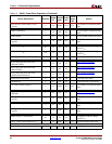
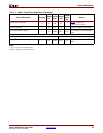
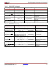
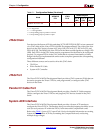
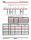
System ACE CF Card — — 1 1 1
Notes:
1. X = Supported.
2. — = Not applicable.
3. Corresponding jumper position is Closed.
4. Corresponding jumper position is Open.
Table 6-1: Configuration Modes (Continued)
Mode
XCONFIG
P72
JTAG
P114
Mode Jumpers
(3,4)
5 -> 6
(M2)
3 -> 4
(M1)
1 -> 2
(M0)


