


x
List of FiguresList of Figures
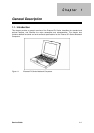
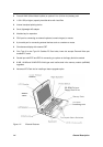
1-1 Extensa 67x Series Notebook Computers................................................................1-1
1-2 External Features......................................................................................................1-4
1-3 External Ports............................................................................................................1-6
1-4 Installing PCMCIA Card Options...............................................................................1-8
3-1 67x Operating Controls and Indicators......................................................................3-1
4-1 Extensa 670 System Architecture Diagram ..............................................................4-5
4-2 M1521 Pin Assignments ...........................................................................................4-6
4-3 M1523 Chip Simplified Block Diagram......................................................................4-8
4-4 M1523 Chip Pinouts..................................................................................................4-9
4-5 M6377 Chip Simplified Block Diagram....................................................................4-11
4-6 M6377 Chip Pinouts................................................................................................4-12
4-7 C&T65550 Chip Pinouts..........................................................................................4-14
4-8 C&T65550 Chip Simplified Block Diagram .............................................................4-15
4-9 TI1130 Chip PCI-to-PC card (16-bit) Pinouts..........................................................4-16
4-10 TI1130 Chip PCI-to-CardBus (32-bit) Pinouts.........................................................4-17
4-11 TI1130 Chip Simplified Block Diagram ...................................................................4-18
4-12 NS87336VJG Chip Pinouts.....................................................................................4-21
4-13 NS87336VJG Chip Simplified Block Diagram.........................................................4-22
4-14 ES1878 Chip Pinouts ..............................................................................................4-23
6-1 Removing/Installing Cables with Locking-Type Connectors .....................................6-3
6-2 Battery Removal/Replacement .................................................................................6-4
6-3 Installing/Removing PCMCIA Options ......................................................................6-5
6-4 Removing the HDD Bay Cover..................................................................................6-6
6-5 Removing/Replacing the Hard Disk Drive Module....................................................6-6
6-6 Removing the Display Hinge Covers.........................................................................6-7
6-7 Removing/Replacing the Keyboard Assembly ..........................................................6-7
6-8 Memory Expansion Removal/Replacement.............................................................6-8
6-9 Removing/Replacing the Heat Sink Assembly.........................................................6-9
6-1 0 Removing/Replacing the CPU Chip .....................................................................6-10
6-1 1 Removing/Replacing a Module ............................................................................6-11
6-1 2 Unplugging the Display Cable ..............................................................................6-12
6-13 Removing the Display Hinge Screws......................................................................6-12
6-14 Removing/Replacing the Top Cover.......................................................................6-13
6-15 Unplugging Cables on FIR/Audio Board .................................................................6-14
6-16 Removing/Replacing the FIR/Audio Board .............................................................6-14