


User’s Manual
BOSCH
- 14/77 -
Revision 1.6TTCAN
11.11.02
manual_about.fm
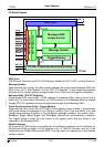
2.3.4.6 Software control of Pin CAN_TX
Four output functions are available for the CAN transmit pin CAN_TX. Additionally to its
default function – the serial data output – it can drive the CAN Sample Point signal to monitor
the CAN_Core’s bit timing and it can drive constant dominant or recessive values. The last two
functions, combined with the readable CAN receive pin CAN_RX, can be used to check the
CAN bus’ physical layer.
The output mode of pin CAN_TX is selected by programming the Test Register bits Tx1 and
Tx0 as described in section 2.3.4.1 on page 11.
The three test functions for pin CAN_TX interfere with all CAN protocol functions. CAN_TX
must be left in its default function when CAN message transfer or any of the test modes Loop
Back Mode, Silent Mode, or No Message RAM Mode are selected.
2.3.4.7 No Message RAM Mode
The CAN_Core can be set in No Message RAM Mode by programming the Test Register bit
NoRAM to
one
. In this mode the TTCAN module operates without the Message RAM.
The IF1 Registers are used as Transmit Buffer. The transmission of the contents of the IF1
Registers is requested by writing the Busy bit of the IF1 Command Request Register to ‘1’.
The IF1 Registers are locked while the Busy bit is set. The Busy bit indicates that the
transmission is pending. The CPU-IFC’s output signal CAN_WAIT_B is disabled (always ‘1’)
in this mode.
As soon the CAN bus is idle, the IF1 Registers are loaded into the CAN_Core’s shift register
and the transmission is started. When the transmission has completed, the Busy bit is reset
and the locked IF1 Registers are released.
A pending transmission can be aborted at any time by resetting the Busy bit in the IF1
Command Request Register while the IF1 Registers are locked. If the CPU has reset the Busy
bit, a possible retransmission in case of lost arbitration or in case of an error is disabled.
The IF2 Registers are used as Receive Buffer. After the reception of a message the contents
of the shift register is stored into the IF2 Registers, without any acceptance filtering.
Additionally, the actual contents of the shift register can be monitored during the message
transfer. Each time a read Message Object is initiated by writing the Busy bit of the IF2
Command Request Register to ‘1’, the contents of the shift register is stored into the IF2
Registers.
In No Message RAM Mode the evaluation of all Message Object related control and status bits
and of the control bits of the IFx Command Mask Registers is turned off. The message
number of the Command request registers is not evaluated. The NewDat and MsgLst bits of
the IF2 Message Control Register retain their function, DLC3-0 will show the received DLC,
the other control bits will be read as ‘0’.
The No Message RAM Mode is a hardware test mode that allows to evaluate the TTCAN IP
RTL code in FPGA types that do not support the TTCAN’s Message RAM structure.