


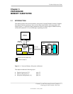
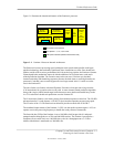

Chapter 3 Processor/Memory Subsystem
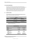
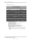
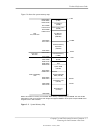
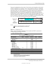
The SPD address map is shown below.
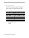
Table 3–1. SPD Address Map (SDRAM DIMM)
Table 3-3.
SPD Address Map (SDRAM DIMM)
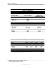
Byte
Description Notes Byte Description Notes
0 No. of Bytes Written Into EEPROM [1] 25 Min. CLK Cycle Time at
CL X-2
[7]
1 Total Bytes (#) In EEPROM [2] 26 Max. Acc. Time From
CLK @ CL X-2
[7]
2 Memory Type 27 Min. Row Prechge. Time [7]
3 No. of Row Addresses On DIMM [3] 28 Min. Row Active to Delay [7]
4 No. of Column Addresses On DIMM 29 Min. RAS to CAS Delay [7]
5 No. of Module Banks On DIMM 30, 31 Reserved
6, 7 Data Width of Module 32..61 Superset Data [7]
8 Voltage Interface Standard of DIMM 62 SPD Revision [7]
9 Cycletime @ Max CAS Latency (CL) [4] 63 Checksum Bytes 0-62
10 Access From Clock [4] 64-71 JEP-106E ID Code [8]
11 Config. Type (Parity, Nonparity, etc.) 72 DIMM OEM Location [8]
12 Refresh Rate/Type [4] [5] 73-90 OEM’s Part Number [8]
13 Width, Primary DRAM 91, 92 OEM’s Rev. Code [8]
14 Error Checking Data Width 93, 94 Manufacture Date [8]
15 Min. Clock Delay [6] 95-98 OEM’s Assembly S/N [8]
16 Burst Lengths Supported 99-125 OEM Specific Data [8]
17 No. of Banks For Each Mem. Device [4] 126 Intel frequency check
18 CAS Latencies Supported [4] 127 Reserved
19 CS# Latency [4] 128-131 Compaq header “CPQ1” [9]
20 Write Latency [4] 132 Header checksum [9]
21 DIMM Attributes 133-145 Unit serial number [9] [10]
22 Memory Device Attributes 146 DIMM ID [9] [11]
23 Min. CLK Cycle Time at CL X-1 [7] 147 Checksum [9]
24 Max. Acc. Time From CLK @ CL X-1 [7] Reserved [9]
NOTES:
[1] Programmed as 128 bytes by the DIMM OEM
[2] Must be programmed to 256 bytes.
[3] High order bit defines redundant addressing: if set (1), highest order RAS# address must be
re-sent as highest order CAS# address.
[4] Refer to memory manufacturer’s datasheet
[5] MSb is Self Refresh flag. If set (1), assembly supports self refresh.
[6] Back-to-back random column addresses.
[7] Field format proposed to JEDEC but not defined as standard at publication time.
[8] Field specified as optional by JEDEC but required by this system.
[9] Compaq usage. This system requires that the DIMM EEPROM have this
space available for reads/writes.
[10] Serial # in ASCII format (MSB is 133). Intended as backup identifier in case vender data is
invalid.
Can also be used to indicate s/n mismatch and flag system adminstrator of possible system
Tampering.
[11] Contains the socket # of the module (first module is “1”). Intended as backup identifier (refer to
note [10]).
Compaq Evo and Workstation Personal Computers
Featuring the Intel Pentium 4 Processor
Second Edition - January 2003
3-6