. . . . .
PMC/PCI INTERFACE
PMC Module Installation
10004281-02 CC1000dm User’s Manual 3-3
Timing
The module interface transfers data between the PCI and local memory at burst data
rates. When two modules are installed, they both contend for ownership of a common
bus, which may reduce the individual performance of each module. Specific transfer
rates to the PCI bus are dependent on the module design.
Many PMC modules also incorporate a bridge chip between their PCI and local busses,
essentially creating two bridges that must be crossed to complete a cycle. Often, the
second bridge is a source of long delays due to the associated bus acquisition latency.
Initialization and time-out values should be set up to accommodate any additional
latency.
Interrupts
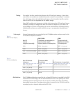
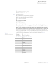
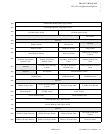
External interrupts that are controlled by the CC1000dm carrier card are routed to the
on-board devices/slots as follows:
Arbitration
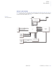
The CC1000dm arbitration control for the on-board PCI devices is provided by the PLX
PCI 6254 PCI-to-PCI bridge. The PCI 6254 arbitrates for use of the primary bus when
initiating upstream transactions and for use of the secondary bus when forwarding
downstream transactions. The primary bus arbiter is external to the PCI 6254, and the
secondary bus is an internal arbiter on the PCI 6254.
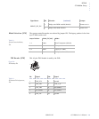
Base PCI
Interrupt
Assignment (secondary):
PMC1/ PMC2
(Transparent, non-transparent, no
system controller modes)
System Controller PCI Interrupt Line:
PMC1
(Legacy mode only)
Non-System Controller
PCI Interrupt Line:
.
.
.
.
.
.
.
.
.
.
.
.
.
.
.
.
.
.
.
.
.
.
.
.
.
.
.
.
.
.
.
.
.
.
.
.
.
.
.
.
.
.
.
.
.
.
.
.
.
.
.
.
INTA INTA (J21, pin 4) INTC (J11, pin 6)
INTB INTB (J21, pin 5) INTD (J11, pin 9)
INTC PLX PCI 6254 (HB6) INTC (J21, pin 6) INTA (J11, pin 4)
INTD INTD (J21, pin 9) INTB (J11, pin 5)
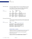
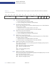
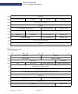
Base cPCI Interrupt
Assignment:
Transparent Mode
(secondary): Non-Transparent or Legacy Mode:
.
.
.
.
.
.
.
.
.
.
.
.
.
.
.
.
.
.
.
.
.
.
.
.
.
.
.
.
.
.
.
.
.
.
.
.
.
.
.
.
.
.
.
.
.
.
.
.
.
.
.
.
INTA (J1, pin A3) INTA INTA (PCI 6254 primary side)
INTB (J1, pin B3) INTB –
INTC (J1, pin C3) INTC –
INTD (J1, pin E3) INTD –
Ta b l e 3 - 3 :
PMCx Interrupt Mapping
Ta b l e 3 - 4 :
cPCI Interrupt Mapping


