


. . . . .
PMC/PCI INTERFACE
PCI Identification Values
10004281-02 CC1000dm User’s Manual 3-11
. . . . . . . . . . . . . . . . . . . . . . . . . . . . . . . . . . . . . . . . . . . . . . . . . . . .
PCI IDENTIFICATION VALUES
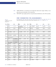
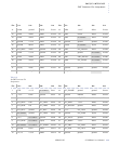
Each CC1000dm configuration has a unique set of identification values. The base
address for these values is determined by the CC1000dm’s location in the cPCI rack and
the baseboard. The standard PCI hex offsets are:
Vendor ID 00
16
Device ID 02
16
Subsystem Vendor ID 2C
16
Subsystem ID 2E
16
All of these values are two bytes wide (half-word). Please refer to the PLX PCI 6254
data book for more information. The following table lists the identification values for
the different CC1000dm configurations:
. . . . . . . . . . . . . . . . . . . . . . . . . . . . . . . . . . . . . . . . . . . . . . . . . . . .
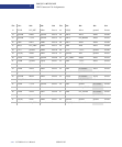
JTAG HEADERS
Each processor PMC slot has a 10-pin debug header (see Fig. 2-5). These headers are
located at JP1 (PMC1) and JP2 (PMC2) to provide easy access to the following signals
in
Table 3-8:
The signals for the JTAG header are defined as follows:
TCK:
Test Clock Input is clock state information and test data into and out of PMC slots dur-
ing the test access port (TAP) operation. Scan data is latched at the rising edge of this
signal.
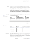
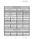
Vendor
ID (hex):
Device
ID (hex):
Subsystem
Vendor ID (hex):
Subsystem
Device ID (hex): PCI 6254 Bridge Mode:
.
.
.
.
.
.
.
.
.
.
.
.
.
.
.
.
.
.
.
.
.
.
.
.
.
.
.
.
.
.
.
.
.
.
.
.
.
.
.
.
.
.
.
.
.
.
.
.
.
3388 20 – – Transparent
21 1223 3A Non-transparent
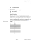
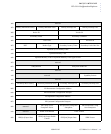
Pin: Signal: Pin: Signal:
.
.
.
.
.
.
.
.
.
.
.
.
.
.
.
.
.
.
.
.
.
.
.
.
.
.
.
.
.
1TCK 2ground
3TDO 45V (fused)
5TMS
6 no connect
7 no connect 8 no connect
9TDI 10ground
Ta b l e 3 - 7 :
PCI Identification Values
Ta b l e 3 - 8 :
Debug Header Pin
Assignments (JP1, JP2)