


. . . . .
CARRIER CARD BUS INTERFACE
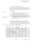
CC1000dm Control Signals
10004281-02 CC1000dm User’s Manual 4-5
. . . . . . . . . . . . . . . . . . . . . . . . . . . . . . . . . . . . . . . . . . . . . . . . . . . .
CC1000DM CONTROL SIGNALS
Both the primary (cPCI) and secondary (PMC) sides of the PCI bridge can be selected for
either 3.3 volt or 5 volt signaling. Refer to the PCI Local Bus Specification, Revision 2.3
for details on these signals. All signals are bi-directional unless otherwise stated. This is
described as follows:
. . . . . . . . . . . . . . . . . . . . . . . . . . . . . . . . . . . . . . . . . . . . . . . . . . . .
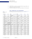
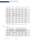
BACKPLANE CONNECTOR PIN ASSIGNMENTS
The tables in this section list the CC1000dm backplane signals. Connectors J1 and J2
provide CompactPCI bus signals (see specification for details). The pin assignments for
connectors J3 and J5 are compatible with the Motorola MCP/MCPN750 board. All sig-
nals are bi-directional unless stated otherwise.
Signal: Description:
.
.
.
.
.
.
.
.
.
.
.
.
.
.
.
.
.
.
.
.
.
.
.
.
.
.
.
.
.
.
.
.
.
.
.
.
.
.
.
.
.
.
.
.
.
.
.
.
.
.
.
.
p_vio PRIMARY INTERFACE I/O VOLTAGE. If a device on the primary PCI bus uses 5 volt
signaling, then p_vio is configured for 5 volt signaling. If the device uses 3.3 volt
signaling, then p_vio is configured for 3.3 volt signaling.
The primary side 3.3 V/5 V operation is controlled by the CompactPCI VIO.
s_vio SECONDARY INTERFACE I/O VOLTAGE. If a device on the secondary PCI bus uses
5 volt signaling, then s_vio is configured for 5 volt signaling. If the device uses 3.3
volt signaling, then s_vio is configured for 3.3 volt signaling.
The secondary side 3.3 V/5 V operation is controlled by a hardware jumper on the
carrier card (refer to page 2-7).
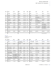
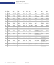
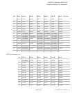
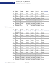
Pin: Row Z: Row A: Row B: Row C: Row D: Row E: Row F:
.
.
.
.
.
.
.
.
.
.
.
.
.
.
.
.
.
.
.
.
.
.
.
.
.
.
.
.
.
.
.
.
.
.
.
.
.
.
.
.
.
.
.
.
.
.
.
.
.
.
.
.
.
.
.
.
.
.
.
.
.
.
.
1 ground +5V -12V no connect +12V +5V ground
2ground
no connect +5V no connect no connect no connect ground
3 ground INTA* INTB* INTC* +5V INTD* ground
4ground
no connect Healthy VIO no connect no connect ground
5ground
no connect no connect RST* ground GNT* ground
6 ground REQ*
PCI_present
1
+3.3V CLK AD31 ground
7 ground AD30 AD29 AD28 ground AD27 ground
8 ground AD26 ground VIO AD25 AD24 ground
9 ground C/BE3* IDSEL
2
AD23 ground AD22 ground
10 ground AD21 ground +3.3V AD20 AD19 ground
Ta b l e 4 - 2 :
Control Signals
N o t e :
The 66 MHz PCI operation
requires 3.3 V signaling.
Ta b l e 4 - 3 :
J1 Connector Pin Assignments