


85
CHAPTER 4 I/O PORTS
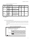
■
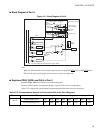
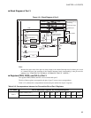
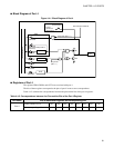
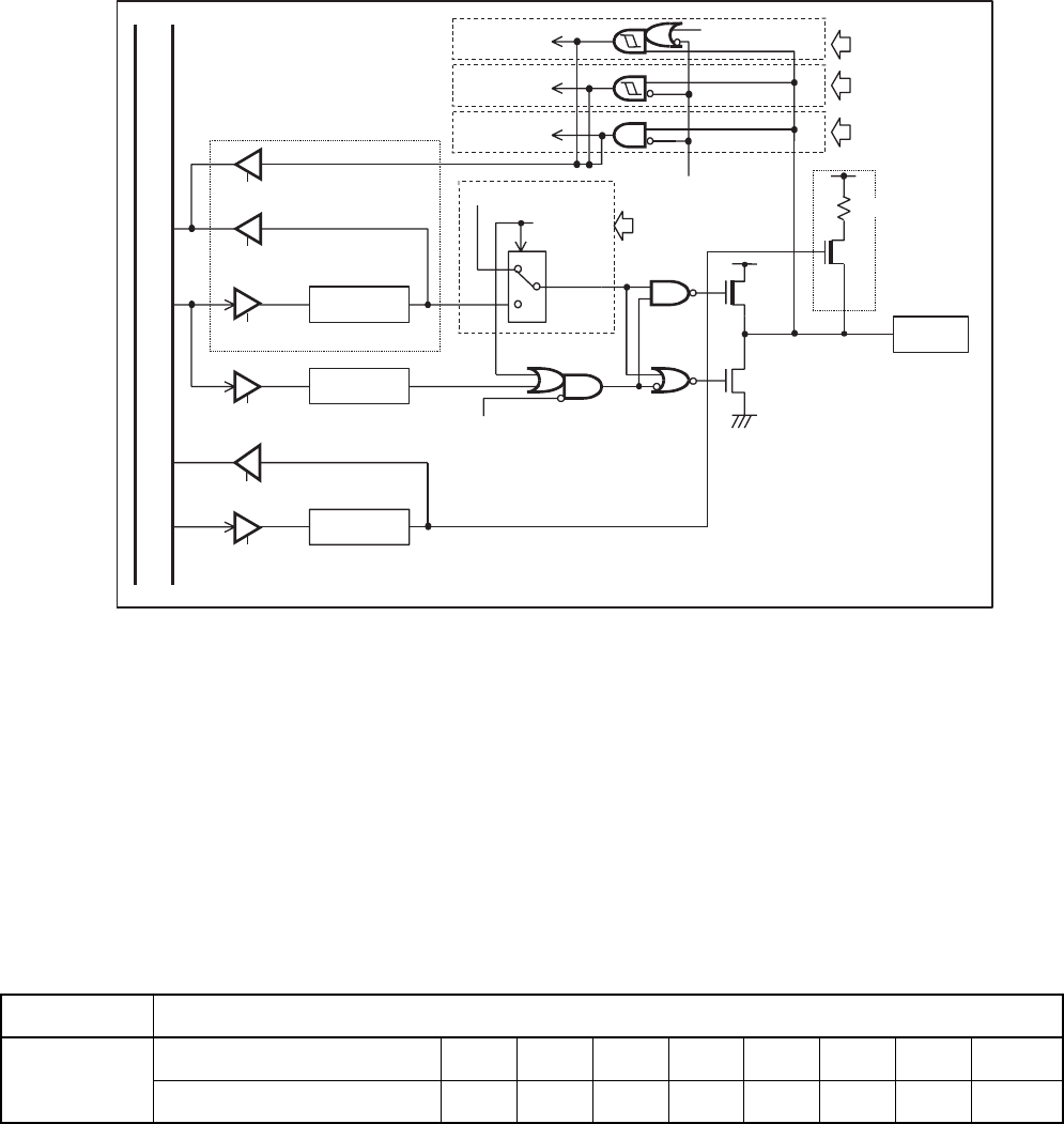
Block Diagram of Port 3
Figure 4.3-1 Block Diagram of Port 3
Note:
Because the value states of the pins are always input to the external interrupt circuit, when a pin is used
as a normal I/O port, the operation of the external interrupt circuit corresponding to the pin must be
inhibited. See "CHAPTER 10 EXTERNAL INTERRUPT CIRCUIT 1 (EDGE) ".
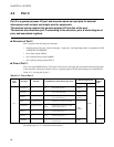
■
Registers PDR3, DDR3, and PUL3 of Port 3
The registers PDR3, DDR3, and PUL3 are associated with port 3.
The bits of these registers correspond to the pins of port 3 in one-to-one correspondence.
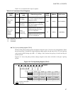
Table 4.3-2 tabulates the correspondence between the pins and the bits of port 3 registers.
DDR
Pch
Nch
PDR
PUL
Internal data bus
PDR read
PDR write
PDR read
(when read-modify-write is
performed)
Output latch
DDR write
PUL read
PUL write
External
interrupt
Input to
peripheral
Input to
peripheral
Output from peripheral
Output
from
peripheral
enable
Stop mode
(SPL = 1)
Output occurring
from peripheral
External interrupt
enable
External interrupt
occurring
Hysteresis input
CMOS input
Pull-up resistor
Pins
Stop mode
(SPL = 1)
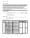
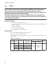
Table 4.3-2 Correspondence between the Pins and the Bits of Port 3 Registers
Port name Bits of associated registers and corresponding pins
Port 3
PDR3, DDR3, PUL3 bit7 bit6 bit5 bit4 bit3 bit2 bit1 bit0
Pin corresponding to bit P37 P36 P35 P34 P33 P32 P31 P30