


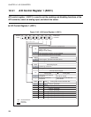

267
CHAPTER 12 A/D CONVERTER
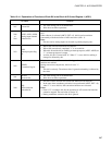
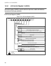
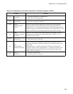
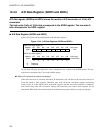
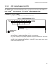
Table 12.4-1 Explanation of Functions of Each Bit in the Bits in A/D Control Register 1 (ADC1)
Bit name Function
bit7 Unused bit
• The value during read is not determined.
• Write does not affect operations.
bit6
to
bit4
ANS2, ANS1, ANS0:
Analog input channel
selection bits
This bit is used to select which pin to be used as an analog input from AN0 to
AN7.
When software is activated (ADC2: EXT = 0), this bit can be rewritten
concurrently with the activation of A/D conversion (AD = 1).
Note:
Pins not used as analog inputs can be used as general-purpose ports.
bit3
ADI:
Interrupt request flag
bit
• When A/D conversion functions are enabled:
• When A/D conversion is completed, "1" is set to this bit.
• When this bit and the bit for enabling an interrupt request (ADC2: ADIE) are
"1", an interrupt request is output.
• At write, this bit is cleared with "0". When "1" is set to this bit, nothing is
changed or affected by this.
bit2
ADMV:
Convertion flag bit
This bit indicates that A/D conversion is being performed, when A/D conversion
functions are enabled.
During conversion (comparison), this bit is set to "1".
Note:
This bit is read-only. The written value is ignored and nothing is affected by
the value.
bit1
RESV0:
Reserved bit
• The value during read is not determined.
• Write does not affect operations.
bit0
AD:
A/D conversion
activation bit
• This bit is used to activate A/D conversion functions with software.
• In the state where continuous activation is not performed (ADC2: EXT = 0),
when "1" is set to this bit, A/D conversion functions are activated.
Notes:
• Even if "0" is written to this bit, the operation of A/D conversion functions
cannot be stopped. The read value is always "0".
• During continuous activation, this bit is ignored.