


91
CHAPTER 4 I/O PORTS
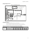
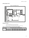
■
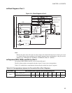
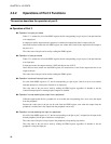
Block Diagram of Port 4
Figure 4.4-1 Block Diagram of Port 4
■
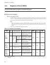
Registers of Port 4
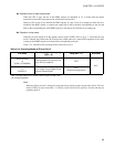
The registers PDR4, DDR4, and OUT4 are associated with port 4.
The bits of these registers correspond to the pins of port 4 in one-to-one correspondence.
Table 4.4-2 tabulates the correspondence between the pins and the bits of the port 4 registers.
DDR
Pch
Nch
PDR
OUT
Internal data bus
PDR read
PDR read
(when read-modify-write is
performed)
Output latch
PDR write
DDR write
Stop mode
(SPL = 1)
OUT read
OUT write
A/D converter
channel select
To A/D
converter's
analog input
A/D converter enable bit
Pins
Stop mode (SPL = 1)
DDR read
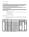
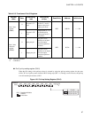
Table 4.4-2 Correspondence between the Pins and the Bits of the Port 4 Register
Port name Bits of associated registers and corresponding pins
Port 4
PDR4, DDR4, OUT4 bit7 bit6 bit5 bit4 bit3 bit2 bit1 bit0
Pin corresponding to bit - - - - P43 P42 P41 P40