


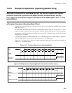
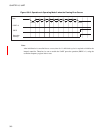
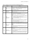

317
CHAPTER 14 8-BIT SERIAL I/O
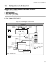
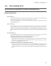
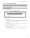
14.3 Pins of 8-Bit Serial I/O
8-bit serial I/O pins include P32/UI/SI, P31/UO/SO, and P30/UCK/SCK pins.
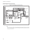
■ Pins of 8-bit Serial I/O
● P32/UI/SI pin
The P32/UI/SI pin functions as the general-purpose I/O port (P32). It also functions as the serial data input
pin (SI) of the 8-bit serial I/O or as the serial data input pin (UI) of the UART.
When using the P32/SI pin as the SI pin, set the P32/UI/SI pin to "input port" with the port direction
register (DDR3: bit2 = 0).
● P31/UO/SO pin
The P31/UO/SO pin functions as the general-purpose I/O port (P31). It also functions as the serial data
output pin (SO) function of the 8-bit serial I/O or as the serial data output pin (UO) function of the UART.
When the serial data output is allowed (SMR: SOE = 1), the P31/UO/SO pin automatically becomes an
output pin irrespective of the values in the port direction register (bit1 of DDR3) and functions as the SO
pin.
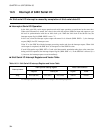
● P30/UCK/SCK pin
The P30/UCK/SCK pin functions as the general-purpose I/O port (P30). It also functions as the shift clock
I/O pin (SCK) of the 8-bit serial I/O or as the shift clock I/O pin (UCK) of the UART.
When using the P30/UCK/SCK pin as the shift clock input pin
When using the SCK pin as the shift clock input pin, set it to "input port" with the port direction register
(DDR3: bit3 = 0) and prohibit shift clock output (SMR: SCKE = 0). In this case, be sure to select the
external shift clock (SMR: CKS1, CKS0 = 11
B
).
When using the P30/UCK/SCK pin as the shift clock output pin
When the shift clock output is allowed (SMR: SCKE = 1), the P30/UCK/SCK pin automatically becomes
an output pin irrespective of the values in the port direction register (DDR3: bit0) and functions as the
SCK output pin. In this case, be sure to select an internal shift clock (when SMR: CKS1, CKS0 are not
11
B
).