


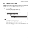
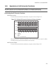
266
CHAPTER 12 A/D CONVERTER
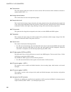
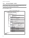
12.4.1 A/D Control Register 1 (ADC1)
A/D control register 1 (ADC1) is used to set the enabling and disabling functions of the
A/D converter, select an analog input, and check the status.
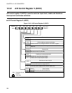
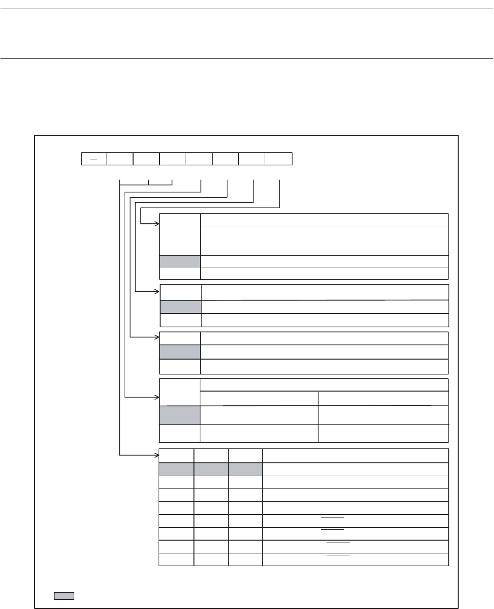
■ A/D Control Register 1 (ADC1)
Figure 12.4-2 A/D Control Register 1 (ADC1)
AD
0
1
RESV0
0
1
ADMV
0
1
ADI
0
1
ANS2 ANS1 ANS0
000
001
010
011
100
101
110
111
bit7 bit6 bit5 bit4 bit3 bit2 bit1 bit0
0030
H
ANS2 ANS1
ANS0
ADI
ADMV RESV0 AD -0000000
B
R/W R/W R/W R/W R R/W R/W
R/W : Readable/Writable
R : Read only
: Initial value
Address Initial value
A/D conversion activation bit
This bit is enabled only when software is activated
(ADC2: EXT = 0).
Always 0 for at reading.
A/D conversion functions are not activated.
A/D conversion functions are activated.
Reserved bit
Not changed. This does not affect others.
Converting flag bit
Not changed. This does not affect others.
Not during conversion.
During conversion.
Interrupt request flag bit
During read
During write
Conversion has not been
completed.
This bit is cleared.
Analog input channel selection bits
Conversion has been
completed.
Not changed. This does not
affect others.
AN0 pin (P40/AN0)
AN1 pin (P41/AN1)
AN2 pin (P42/AN2)
AN3 pin (P43/AN3)
AN4 pin (P00/INT20/AN4)
AN5 pin (P01/INT21/AN5)
AN6 pin (P02/INT22 /AN6)
AN7 pin (P03/INT23 /AN7)