


Datasheet 21
Electrical Specifications
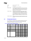
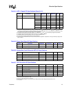
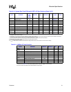
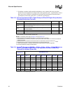
T
low
BCLKp Low Time 266 1.69 1.88 2.06 ns Figure 2-1
4
T
period
BCLKp Period 333 3.0 ns Figure 2-1
T
skew
System Clock Skew 333 60 ps
f
BCLK
BCLKp Frequency 333 333 333 MHz Figure 2-1
T
jitter
BCLKp Input Jitter 333 50 ps Figure 2-1
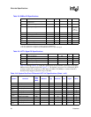
3
T
high
BCLKp High Time 333 1.35 1.5 1.65 ns Figure 2-1
4
T
low
BCLKp Low Time 333 1.35 1.5 1.65 ns Figure 2-1
4
T
rise
BCLKp Rise Time All 333 500 667 ps Figure 2-1 20–80%
T
fall
BCLKp Fall Time All 333 500 667 ps Figure 2-1 20–80%
V
PP
Minimum Input Swing All 600 mV Figure 2-1
6
NOTES:
1. The system clock skew is ±100 ps.
2. Measured on cross point of rising edge of BCLKp and falling edge of BCLKn. Long term jitter is defined as peak-to-peak variation measured by
accumulating a large number of clock cycles and recording peak-to-peak jitter.
3. Cycle-to-cycle jitter is defined as peak-to-peak variation measured over 10000 cycles peak-to-peak jitter.
4. Measured on cross point of rising edge of BCLKp and falling edge of BCLKn.
5. The system clock skew is ±60 ps.
6. V
PPmin
is defined as the minimum input differential voltage which will cause no increase in the clock receiver timing.
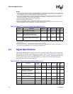
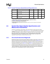
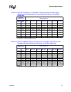
Table 2-11. SMBus AC Specifications
Symbol Parameter Minimum Maximum Unit Notes
f
SMSC
SMSC Clock Frequency 100 kHz
T
SMSC
SMSC Clock Period 10 µs
t
high
SMSC Clock High Time 4.0 µs
1
NOTES:
1. Please refer to Figure 2-2 for the Standard Microsystems Corporation (SMSC)* clock waveform.
t
low
SMSC Clock Low Time 4.7 µs
1
t
rise
SMSC Clock Rise Time 1.0 µs
1
t
fall
SMSC Clock Fall Time 0.3 µs
1
t
VALID
SMBus Output Valid Delay 1.0 µs
t
SU
SMBus Input Setup Time 250 ns
t
HLD
SMBus Input Hold Time 0 ns
t
FREE
Bus Free Time 4.7 µs
2
2. Bus Free Time is the minimum time allowed between request cycles.
Table 2-10. System Bus Clock Differential HSTL AC Specifications (Sheet 2 of 2)
Symbol Parameter
System
Bus
Clock
(MHz)
Minimum Typ Maximum Unit Figure Notes