32 Datasheet
Electrical Specifications
2.7 Itanium
®
2 Processor System Bus Clock and
Processor Clocking
The BCLKn and BCLKp inputs control the operating frequency of the Itanium 2 processor system
bus interface. All Itanium 2 processor system bus timing parameters are specified with respect to
the falling edge of BCLKn and rising edge of BCLKp. The Itanium 2 processor core to bus ratio
must be configured during system reset by using the A[21:17]# pins (see Table 2-25). The value on
these pins during the system reset sequence determines the multiplier that the PLL will use for the
internal core clock. Because the A[21:17]# signals pins have different uses after a system reset is
complete, these signals must be multiplexed for configuration during reset and for normal use after
reset. See the Intel
®
Itanium
®
2 Processor Hardware Developer’s Manual for complete
information on Itanium 2 processor system bus clock and processor clocking.
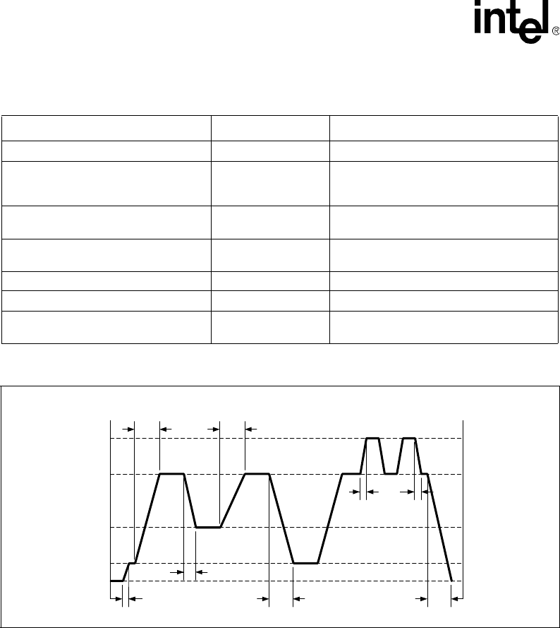
Table 2-24. Processor Power States
State Transition Ramp Rate Comment
Zero to 1st Power State (A) 10 μs Off state to initial power on.
1st Power State to 2nd Power State (B) 10 μs 1st power state is defined as the system
minimum operating load. Fastest power up
sequence.
2nd Power State to 3rd Power State (C) 10 μs 2nd power state is defined as 75% of full
power.
3rd Power State to 2nd Power State (D) 10 μs 3rd power state is defined as 40% of full
power.
2nd Power State to 1st Power State (E) 10 μs Typical fast power down to initial power on.
Normal Operating Range (F) 100 A/μs max Defined as 75% to 100% of full power.
Thermal Trip (G) 1ns ±250 ps or one
processor core cycle.
Processor over temperature condition
emergency shutdown.
Figure 2-5. Processor Full, Normal and Low Power Mode with Timings
000672b
5A
40A 40A
5A
0A
75A
100A 100A
75A
0A
Current Level Current Level
A
B
C
D
E
FF
G


