Datasheet 91
A Signals Reference
This appendix provides an alphabetical listing of all Itanium 2
processor system bus signals. The
tables at the end of this appendix summarize the signals by direction: output, input, and I/O.
For a complete pinout listing including processor specific pins, please refer to Chapter 3, “Pinout
Specifications.”
A.1 Alphabetical Signals Reference
A.1.1 A[49:3]# (I/O)
The Address (A[49:3]#) signals, with byte enables, define a 2
50
Byte physical memory address
space. When ADS# is active, these pins transmit the address of a transaction. These pins are also
used to transmit other transaction related information such as transaction identifiers and external
functions in the cycle following ADS# assertion. These signals must connect the appropriate pins
of all agents on the Itanium 2 processor system bus. The A[49:27]# signals are parity-protected by
the AP1# parity signal, and the A[26:3]# signals are parity-protected by the AP0# parity signal.
On the active-to-inactive transition of RESET#, the processors sample the A[49:3]# pins to
determine their power-on configuration.
A.1.2 A20M# (I)
A20M# is ignored in the Itanium 2 processor system environment.
A.1.3 ADS# (I/O)
The Address Strobe (ADS#) signal is asserted to indicate the validity of the transaction address on
the A[49:3]#, REQ[5:0]#, AP[1:0]# and RP#pins. All bus agents observe the ADS# activation to
begin parity checking, protocol checking, address decode, internal snoop, or deferred reply ID
match operations associated with the new transaction.
A.1.4 AP[1:0]# (I/O)
The Address Parity (AP[1:0]#) signals can be driven by the request initiator along with ADS# and
A[49:3]#. AP[1]# covers A[49:27]#, and AP[0]# covers A[26:3]#. A correct parity signal is high if
an even number of covered signals are low and low if an odd number of covered signals are low.
This allows parity to be high when all the covered signals are high.
A.1.5 ASZ[1:0]# (I/O)
The ASZ[1:0]# signals are the memory address-space size signals. They are driven by the request
initiator during the first Request Phase clock on the REQa[4:3]# pins. The ASZ[1:0]# signals are
valid only when REQa[2:1]# signals equal 01B, 10B, or 11B, indicating a memory access
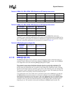
transaction. The ASZ[1:0]# decode is defined in Table A-1.


