MPCBL0010 SBC—Telecom Clock
Intel NetStructure
®
MPCBL0010 Single Board Computer
Technical Product Specification October 2006
162 Order Number: 304120
12.2 Interface Description
12.2.1 AdvancedTCA Backplane Interface
The redundant reference clock CLK1A /CLK1B (8 kHz), and CLK2A/CLK2B (19.44 MHz),
are connected from the AdvancedTCA* backplane. These signals use Multipoint-Low
Voltage Differential Signaling (M-LVDS). Since only very short stub lengths are allowed
with these signals, M-LVDS to Low Voltage Transistor-Transistor Logic (LV-TTL) level
converters have to been placed near to the backplane connectors. Two pairs of the
redundant clocks are connected to the telecom clock module inputs.
12.2.2 AdvancedMC Interface
The telecom clock module supports two AdvancedMC modules. Each module has one
clock input (CLKA), and one clock output (CLKB). These clocks have LVDS signal levels
that have to be realized in point-to-point connection. These clocks can be disabled
separately for cases when they are not needed. The AdvancedMC clock output, which is
used to pass a recovered line clock, enables the system to use a line interface as a
synchronization source. The clock frequency of this interface is unchanged and the
clocks are passed to CLK3A/CLK3B on the AdvancedTCA backplane. These inputs can
be left open if an AdvancedMC module is not installed.
12.2.3 Reset/Interrupt Interface
The telecom clock module has to be reset once after power-up to define the default
state in all devices on the module. The interrupt signals (open drain, active low) when
any alarm occurs.
12.2.4 LPC Interface
The LPC interface is used to configure the telecom clock module. It is also used to
check the status of the configuration information saved in the I
2
C EEPROM.
12.3 Function Description
12.3.1 Redundant Reference Clock Selection
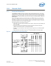
CLK1A/CLK1B (8 kHz) and CLK2A/CLK2B (19.44 MHz) are derived from the
AdvancedTCA backplane. The signal level is converted from M-LVDS into LVTTL. One of
these redundant pairs can be selected as a redundant source pair. Both signals of the
pair are supervised to detect loss of clock. Frequency accuracy is not supervised. If the
selected clock fails (more than about two clock cycles), a loss of signal (LOS) alarm is
declared via an interrupt and the reference clock is switched to another one in a hitless-
switch manner.
The selected clock is used as the phase lock loop (PLL) reference clock on which the
generated clocks synchronize. The PLL unlock and/or holdover alarm can also be used
as a cause for switchover.
12.3.2 PLL Clock Generation
The PLL supports many different frequencies for flexibility. The following frequencies
can be selected individually per AdvancedMC module:
•8 kHz
•1.544 MHz


