MPCBL0010 SBC—Error Messages
Intel NetStructure
®
MPCBL0010 Single Board Computer
Technical Product Specification October 2006
90 Order Number: 304120
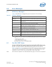
Table 61. Bootblock Initialization Code Checkpoints
Checkpoint Description
Before D1
Early chipset initialization is done. Early super I/O initialization is done, including RTC and
keyboard controller. NMI is disabled.
D1
Perform keyboard controller BAT test. Check if waking up from power management suspend
state. Save power-on CPUID value in scratch CMOS.
D0 Go to flat mode with 4 GByte limit and GA20 enabled. Verify the bootblock checksum.
D2
Disable CACHE before memory detection. Execute full memory sizing module. Verify that flat
mode is enabled.
D3
If memory sizing module not executed, start memory refresh and do memory sizing in
Bootblock code. Do additional chipset initialization. Re-enable CACHE. Verify that flat mode is
enabled.
D4 Test base 512 KByte memory. Adjust policies and cache first 8 GBytes. Set stack.
D5
Bootblock code is copied from ROM to lower system memory and control is given to it. BIOS
now executes out of RAM.
D6
Both key sequence and OEM-specific methods are checked to determine if BIOS recovery is
forced. Main BIOS checksum is tested. If BIOS recovery is necessary, control flows to
checkpoint E0.
D7
Restore CPUID value back into register. The Bootblock-Runtime interface module is moved to
system memory and control is given to it. Determine whether to execute serial flash.
D8 The Runtime module is uncompressed into memory. CPUID information is stored in memory.
D9
Store the Uncompressed pointer for future use in PMM. Copying Main BIOS into memory.
Leaves all RAM below 1 MByte Read-Write including E000 and F000 shadow areas but closing
SMRAM.
DA
Restore CPUID value back into register. Give control to BIOS POST (ExecutePOSTKernel). See
Table 62, “POST Code Checkpoints” on page 90 for more information.
E1-E8
EC-EE
OEM memory detection/configuration error. This range is reserved for chipset vendors and
system manufacturers. The error associated with this value may different from one platform to
the next.
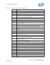
Table 62. POST Code Checkpoints
Checkpoint Description
03
Disable NMI, parity, video for EGA, and DMA controllers. Initialize BIOS, POST, runtime data
area. Also initialize BIOS modules on POST entry and GPNV area. Initialized CMOS as
mentioned in the kernel variable.
04
Check CMOS diagnostic byte to determine if battery power is OK and CMOS checksum is OK.
Verify CMOS checksum manually by reading storage area. If the CMOS checksum is bad,
update CMOS with power-on default values and clear passwords. Initialize status register A.
Initializes data variables that are based on CMOS setup questions. Initializes both the 8259
compatible PICs in the system.
05 Initializes the interrupt controlling hardware (generally PIC) and interrupt vector table.
06
Do R/W test to CH-2 count reg. Initialize CH-0 as system timer. Install the POSTINT1Ch
handler. Enable IRQ-0 in PIC for system timer interrupt. Traps INT1Ch vector to
“POSTINT1ChHandlerBlock.”
08
Initializes the CPU. The BAT test is being done on KBC. Program the keyboard controller
command byte is being done after Auto detection of KB/MS using AMI KB-5.
C0 Early CPU Init Start -- Disable Cache - Init Local APIC.
C1 Set up bootstrap processor information.
C2 Set up bootstrap processor for POST.
C5 Enumerate and set up application predecessors.
C6 Re-enable cache for bootstrap processor.


