


16 SKA4 Baseboard Product Guide
Memory
Main memory resides on an add-in board, called a memory module, designed for the SKA4
baseboard. The memory module contains slots for 16 DIMMs, each of which must be at least
64 MB, and is attached to the baseboard through a 330-pin connector, called the Memory
Expansion Card Connector (MECC). The memory module supports PC-100 compliant registered
ECC SDRAM memory modules. The ECC used for the memory module is capable of correcting
single-bit errors (SBEs) and detecting 100 percent of double-bit errors over one code word. Nibble
error detection is also provided.
System memory begins at address 0 and is continuous (flat addressing) up to the maximum amount
of DRAM installed (exception: system memory is noncontiguous in the ranges defined as memory
holes using configuration registers). The system supports both base (conventional) and extended
memory.
• Base memory is located at addresses 00000h to 9FFFFh (the first 1 MB).
• Extended memory begins at address 0100000h (1 MB) and extends to 3FFFFFFFFh (16 GB),
which is the limit of supported addressable memory. The top of physical memory is a
maximum of 16 GB (to 3FFFFFFFFh).
Memory amounts from 256 MB to 16 GB of DIMM are supported, with a 64/72-bit
four-way-interleaved pathway to main memory, which is also located on the module. Therefore,
data transfers between MADPs and DIMMs is in four-way interleave fashion. Each of the four
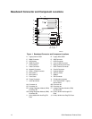
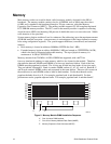
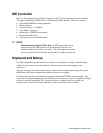
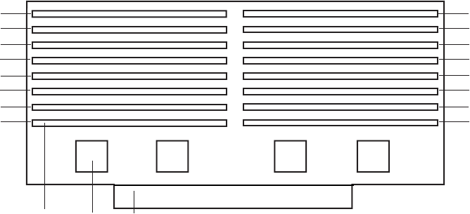
DIMMs must be populated in a bank. The 16 slots are divided into four banks of four slots each.
They are labeled A through D. Bank A contains DIMM sockets A1, A2, A3, and A4. Banks B, C,
and D each contain 4 DIMM sockets and are named in the same fashion. There are silk screens on
the module next to each DIMM socket to label its bank number. For the best thermal results,
populate the banks from A to D. For example, populate bank A and then bank B. For best
performance results, populate adjacent banks. For example, populate bank A and then bank C.
OM09919
A1
A2
A3
A4
B1
B2
B3 B4
C1
C2
C3
C4
D1
D2
D3
D4
XY
Z
Figure 2. Memory Module DIMM Installation Sequence
X. One of sixteen DIMM sockets
Y. One of four Memory Address Data Paths (MADP)
Z. Memory Expansion Card Connector (MECC)