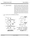
A blinking LED indicates that the load is powered by the
Inverter, not from the Utility. The "BYPASS" LED will be
illuminated Green if the Utility is within acceptable voltage
and frequency limits as specified by the 50/60 Hz DIP switch
setting. Yellow indicates the Utility is not within proper limits.
Red indicates the utility is out of tolerance, do not transfer to
bypass. Not illuminated indicates that bypass is not
available.
A blinking LED indicates that the load is being powered by
the Utility source and not from the Inverter. Green indicates
the Inverter is ready to power the load. Yellow indicates
Inverter warnings for overload or overload recovery cycle,
thermal DC, and bypass abnormal conditions. Red indicates
the Inverter can not operate properly. LED not illuminated
indicates the inverter is not ON.
An internal power supply is used within the inverter module
which makes several 15 VDC outputs from the -48 VDC
battery input and/or utility AC power through a transformer
and bridge rectifier. The 15 volt outputs are used to power
the AC side electronics ( + & - 15VDC for the control circuits,
one +15 VDC output to operate the "master" inverters half
bridge driver), and a second +15 VDC output to operate the
"slave" inverters half bridge driver. Battery side electronics
(hysteretic battery booster and microprocessor) also
requires + & - 15 VDC.
The power supply is a discontinuous mode "Flyback" supply,
that is, the current in the "Flyback" transformer is zero at the
beginning of every switching cycle. The supply was
designed to produce an output power of 20 watts from D.C.
input voltages ranging from 35 VDC to 80 VDC. Control of
this supply is by an industry standard UC3842AN current
mode control PWM chip operating at 100 kHz. The +15 VDC
output on the Battery side (D.C.) is the regulated voltage.
Tight coupling of the transformer ensures that all other
outputs are reasonably close to 15 volts. Within the
UC3842AN integrated circuit, the voltage error amplifier
positive input terminal is set at one half of the chip's
reference (+5.00 volts). So the negative input terminal (VFB)
must also be at +2.50 volts. A 2490 ohm resistor is
connected from the VFB terminal to ground (1.00 mA.) To
obtain +15 VDC, we need 12.5 volts across a resistor at 1.0
mA, or 12,500ohms. A 12400 ohm resistor was used and the
+15 VDC is actually 14.95 volts.
3.1.6.1 Supply Description
3.1.6 Power Supply
3.1.5.2 “Inverter”
3.1.5.1 “Bypass”
86-153061-00 3 — 9Theory of Operation
Owner’s Manual


