6 - 15 6 - 15
MELSEC-Q
6 DATA COMMUNICATION USING THE NON PROCEDURE PROTOCOL
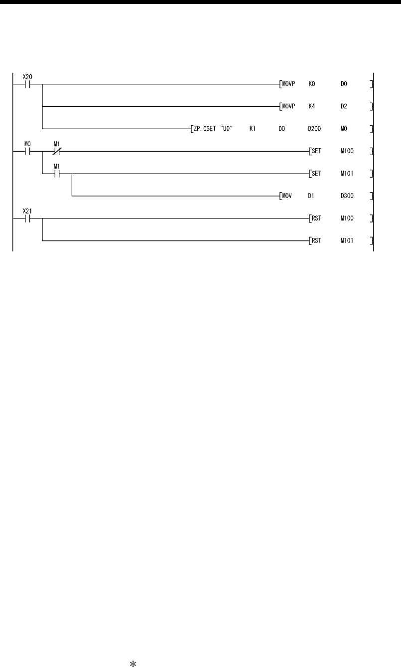
The following is a program example of clearing the reception data by the
dedicated instruction "CSET."
Set the execution type
Set the request type
(Reception data clear)
Execute the reception
data clear
Normal completion
Abnomal completion
Reset the complete flag b
y
external command
(3) Receive data clear procedure using FROM/TO instruction
Write and read the buffer memory receive data clear request area (addresses A8
H
/148
H
) using the procedure described below.
When resuming data communications with an external device, resume it after
completing the reception data clear processing with the Q Series C24.
Depending on the data communications system, it may be necessary to restart
data communications with the external device after notifying the external device
from the PLC CPU that resumption of communications is possible.
(Clear Procedure)· ··When the CH1 side interface is used.
(1) Since receive processing, send processing and receive data clear processing
are not being performed, “1” is written to buffer memory address A8H using
the TO instruction for the sequence program.
(2) Receive data clear processing is performed for the Q Series C24’s OS area
(See Section 6.1.2).
(3) When receive data clear processing is completed, the value in buffer memory
address A8H becomes “0.”
The following page shows an example of a program to clear receive data with the
FROM/TO instruction.
Create a program that contains the contacts (user flags, etc.) indicating the
following statuses in the TO instruction.
• Contact when the CHn reception data read request signal (X3/XA) is OFF
• Contact when the CHn reception abnormal detection signal (X4/XB) is OFF
• Contact indicating that send and receive processes are not currently being
performed
• Contact indicating that reception data clear processing is not currently being
performed
1 When the function version A Q Series C24 is used, resume data
communications a further 100 ms after the buffer memory address
A8H/148H value changes from a “1” to a “0.”


