


Chapter 3 Signal Connections
PC-DIO-24/PnP User Manual 3-8
©
National Instruments Corporation
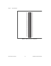
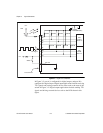
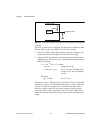
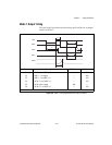
Figure 3-3. DIO Channel Configured for High DIO Power-up State with External Load
Example:
At power up, the board is configured for input and, by default, all DIO
lines are high. To pull one channel low, follow these steps:
1. Install a load (R
L
). Remember that the smaller the resistance, the
greater the current consumption and the lower the voltage.
2. Using the following formula, calculate the largest possible load to
maintain a logic low level of 0.4 V with a minimum reduction to the
DIO drive current.
V = I * R
L
⇒
R
L
= V / I, where:
V= 0.4 V ;Voltage across R
L
I = 46
µ
A + 11
µ
A ;4.6 V across the 100 k
Ω
pull-up
resistor and 11
µ
A max leakage
current
Therefore:
R
L
= 7.0 k
Ω
;0.4V / 57
µ
A
This resistor value, 7.0 k
Ω
, provides a maximum of 0.4 V on the DIO
line at power up. You can substitute smaller resistor values to lower the
voltage or to provide a margin for Vcc variations and other factors.
However, smaller values will draw more current, leaving less drive
current for other circuitry connected to this line. The 7.0 k
Ω
resistor
reduces the amount of logic high source current by 0.4 mA with a 2.8 V
output.
PC-DIO-24/PnP
Digital I/O Line
82C55A
100 kΩ
GND
R
L
+5 V