


Chapter 3 Signal Connections
PC-DIO-24/PnP User Manual 3-10
©
National Instruments Corporation
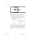
Therefore:
R
L
= 5.6 kΩ ;2.2 V / 39 µA
This resistor value, 5.6 kΩ, provides a minimum of 2.8 V on the DIO
line at power up. You can substitute smaller resistor values but they will
draw more current, leaving less sink current for other circuitry
connected to this line. The 5.6 kΩ resistor will reduce the amount of a
logic low sink current by 0.8 mA with a 0.4 V output.
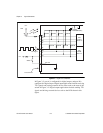
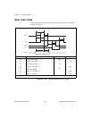
Timing Specifications
This section lists the timing specifications for handshaking with the
PC-DIO-24/PnP. The handshaking lines STB* and IBF synchronize
input transfers. The handshaking lines OBF* and ACK* synchronize
output transfers.
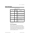
The signals in Table 3-3 are used in the timing diagrams on the
subsequent pages.
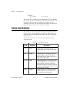
Table 3-3.
Timing Signal Descriptions
Name
Signal
Direction
Description
STB* Input Strobe Input—A low signal on this
handshaking line loads data into the input
latch.
IBF Output Input Buffer Full—A high signal on this
handshaking line indicates that data has
been loaded into the input latch. This is an
input acknowledge signal.
ACK* Input Acknowledge Input—A low signal on this
handshaking line indicates that the data
written from the selected port has been
accepted. This signal is a response from the
external device that it has received the data
from the PC-DIO-24/PnP.
OBF* Output Output Buffer Full—A low signal on this
handshaking line indicates that data has
been written to the selected port.